Hamming Code IC
Table of Contents
Overview
For my course on Very Large Scale Integration (VLSI) design methodologies we had a semester-long, open-ended integrated circuit (IC) design project to complete in groups. I paired myself with a friend and based on his research into Forward Error Correction (FEC) we designed a chip to implement a circuit to generate these codes, with our motivation being that acceleration hardware for this application is needed for future communication standards (200 Gb/s Ethernet).
Since my friend was more invested in the FEC portion, I worked on the supporting circuitry. I did the digital design of these parts and the vast majority of my layout work by hand, making use the methods taught in class to ensure a successful result. All our designs were verified with simulations at each stage of system integration, from the simplest assemblies to final, all-encompassing tests.
In addition to the design of the IC, we also needed to deliver a few presentations on our design and the progress we made over the semester.
Requirements
- Use the TSMC 65 nm technology node, in Cadence
- Occupy less than 2 by 2 mm of die area
- Output Hamming (128, 120, 1) code for input data
- Implement 1:8 interleaving scheme
- Achieve speeds of at least 1 Gb/s
Objectives
- Use less than 5 mW of power at maximum data rate
- Occupy less than 1 by 1 mm of die area
Takeaways
- IC layout is at once similar but also different to PCB layout. Synthsizing entire sections is surreal!
- Agreeing on conventions early on are super important to ensure things move smoothly.
- Designing application specific hardware is truly magnitudes more performant than general purpose hardware.
Background and Motivation
As part of the upcoming 200 Gb/s Ethernet standard Error Correction Codes (ECC) will be required to ensure the reliable transfer of data with a maximum of 1 error per 10^13 bits1 through channels and transceivers which can introduce errors at higher rates. In addition to the error correction codes, interleaving is also a method to harden the communication against errors between endpoints. Since these operations are applied before the data is transmitted, they are called Forward Error Correction, FEC.
Error Correction Codes
The fundamental principle of error correcting codes is that by adding redundant data to payload being transferred, one can correct some number of errors that occur during transfer. This is essentially a compromise between data bandwidth and transmission reliability.
There are several different schemes of error correction codes that can be employed with various benefits and drawbacks. The most basic error correcting code is simply repeating each bit thrice, thus if a single error occurs one can correct it by seeing what is the most common value in a message. This however is only 33% efficient use of bandwidth.
Proper ECC were pioneered by Richard Hamming who devised a scheme to encode four data bits by adding three parity bits (so each transmission was seven). The result allowed a single bit error in the seven to be corrected, and an error of two bits could be detected, but not corrected2. This can be noted as a Hamming (4, 7, 1) scheme.

For our project my partner decided we would use a Hamming (120, 128, 1) code which is being considered for the new 200 Gb/s Ethernet standard3 4. This meant we would take 120 data bits, calculate and append eight parity bits, which would enable one error to be corrected per message. It also allowed for two errors to be detected, but it wouldn’t be able to correct them. This way the downstream device could determine if it was possible or not to repair the detected errors (so long as there aren’t more than three).
Codeword Interleaving
Interleaving is a different way to improve the reliability of a transmission, especially against burst errors5. Unlike ECCs, no redundant data is introduced, rather the data is reshuffled before being sent and then unshuffled when received. Thus if a burst of errors occurs it is generally spread over several payloads which can each correct for it rather than completely corrupting one payload.
Interleaving is generally described by the ratio of shuffling, so a 1:2 ratio means that the first, third, fifth, etc. elements of a set are sent, then the second, fourth, sixth, and so on. For our project we decided to use an 1:8 in our project.
Interleaving Example
A little example using a 1:6 interleaving scheme, with the payload “The quick brown fox jumps over that”. To encode we can write the message in rows of six and then read out by column.
The qu
ick br
own fo
x jump
ed ove
r that

Original   : The quick brown fox jumped over that
Interleaved: Tioxerhcw d eknj t   uohqbfmvauropet
Then applying our burst interference we lose some characters.
Original   : The quick brown fox jumped over that
Interleaved: Tioxerhcw d eknj t   uohqbfmvauropet
Noise      :     -----           ------

Original    (w/ noise): The ----- brown fox ------ over that
Interleaved (w/ noise): Tiox----- d eknj t  ------fmvauropet
Now without interleaving we have lost two entire words and it is impossible for us to recover them. However we have yet undo the interleaving, which can be done the same as interleaving, writing rows of six and reading the columns.
Input : Tiox----- d eknj t  ------fmvauropet

Tiox--
--- d
eknj t
  ----
--fmva
uropet

Output: T-e -ui-k -ro-n-fox j-mp-d -ve- t-at
Thanks to the interleaving the bursts are spread through the message so it is much easier to recover when compared to what would have happened otherwise.
No Inter.  : The ----- brown fox ------ over that
Interleaved: T-e -ui-k -ro-n-fox j-mp-d -ve- t-at
Design
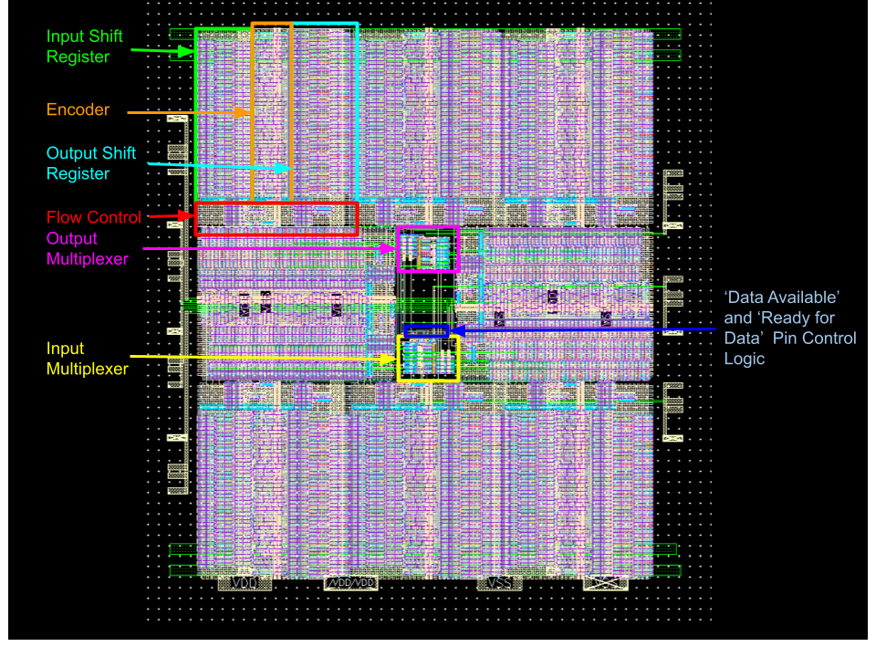
The overall design of our chip was pretty simple there would be a serial stream of data coming in, another out and some digital pins to indicate the state of the chip (if it was read to accept or provide data). Inside there would be eight encoders working in parallel due to the 1:8 interleaving, as well as multiplexers to suit, and some basic logic to summarize the internal flow control state.
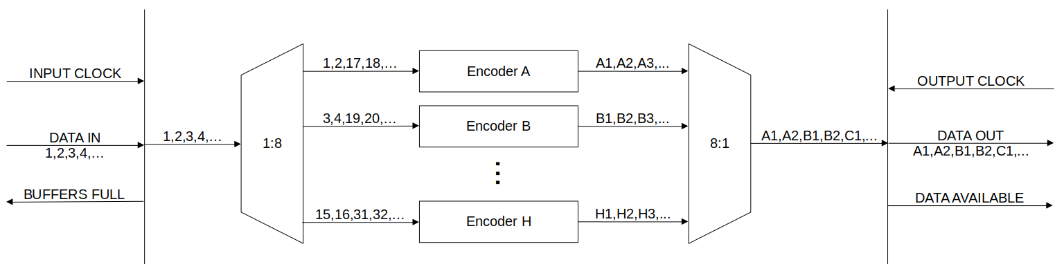
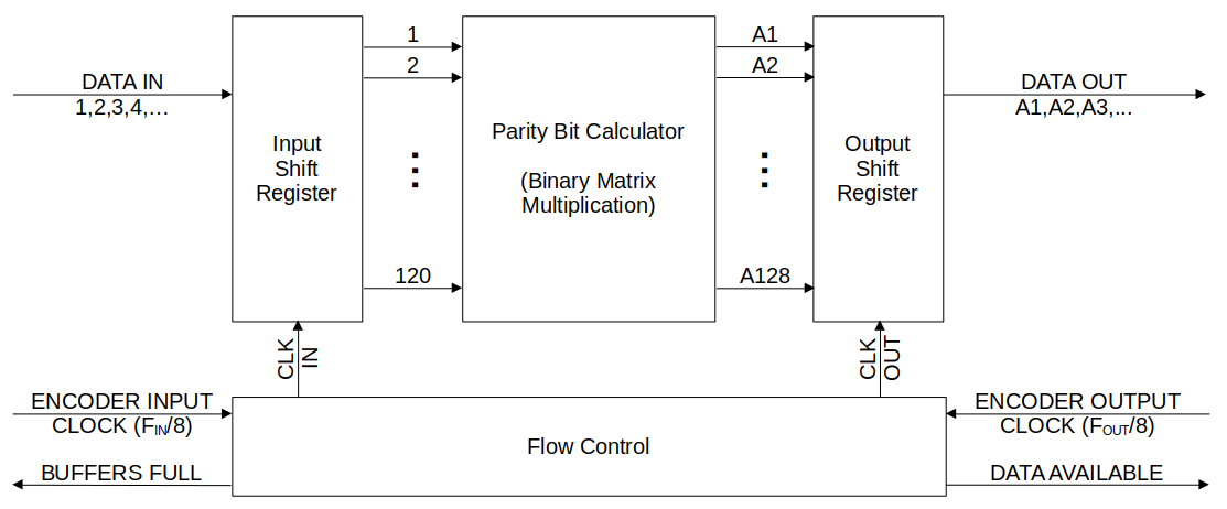
At the heart of each encoder block there was the encoder that would generate the parity bits, supported by shift registers to convert the serial stream into a parallel bus for the logic used in for the encoder and then back into a serial stream. Overseeing each encoder block was a flow control block, the purpose of it was to ensure that the shift registers weren’t overfilled, under-emptied, and that data couldn’t be withdrawn prematurely before the encoding logic settled.
The design work was divided pretty evenly between my partner and I. He worked on the core encoder logic while I designed the surrounding circuitry.
The main challenges I faced in the circuit design was really designing any of the logic, but rather ensuring that our system would be able to operate correctly at frequencies exceeding 1 GHz. To ensure this was met, we performed simulations for each block of our circuit.
Shift Registers
The shift registers were very simple circuits. The input shift registers responsible for converting serial to parallel was just a string of D-Flipflops feeding into one another. To allow data to be loaded in as other data was encoded their outputs were “buffered” using a second bank of flipflops that then actually fed into the encoder block.

As for the parallel to serial shift registers used to output the encoded data, there was a back of flipflops that buffered the data from the encoder block. Their outputs were then fed into another string of flipflops but they had multiplexers to read data in from either the buffer bank (to load in the encoded data) or the flipflops preceding them (to stream the data out).

Since none of the flipflops were fanning out much, large drive strength wasn’t needed. So I elected to use the smallest flipflop variants so they would be more compact when it came to layout.
Multiplexers/Demultiplexers
The multiplexer and demultiplexer used on the input and output respectively were pretty similar to one another. To control the flow of data they actually multiplexed the clock to modules using a shared sub-block that would count the clock cycles and direct the clock (and thus data) into or out of the eight encoder blocks to achieve the 1:8 interleaving.
The multiplexer on the input used a large buffer to fan out the input signal to all the inputs for each encoder block. Only the required encoder block would actually clock in that given bit.

The output demultiplexer used a staged demultiplexer that was synchronized to the output clock multiplexer to forward the output from correct encoder block to the chip output.

Clock Multiplexer
This was a little more than a four bit counter connected to a 1:8 multiplexer for the clock signal. Although we were doing 1:8 interleaving, we were interleaving two bits at a time so we needed to have the clock go twice to each encoder block, hence why a four bit counter was used, with the three most significant bits used for multiplexer selection. The counter incremented on the falling edges of clocks so that the rising edges used elsewhere were properly propagated.

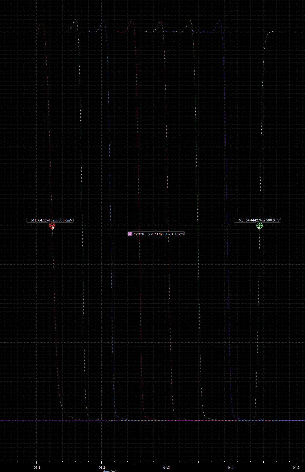
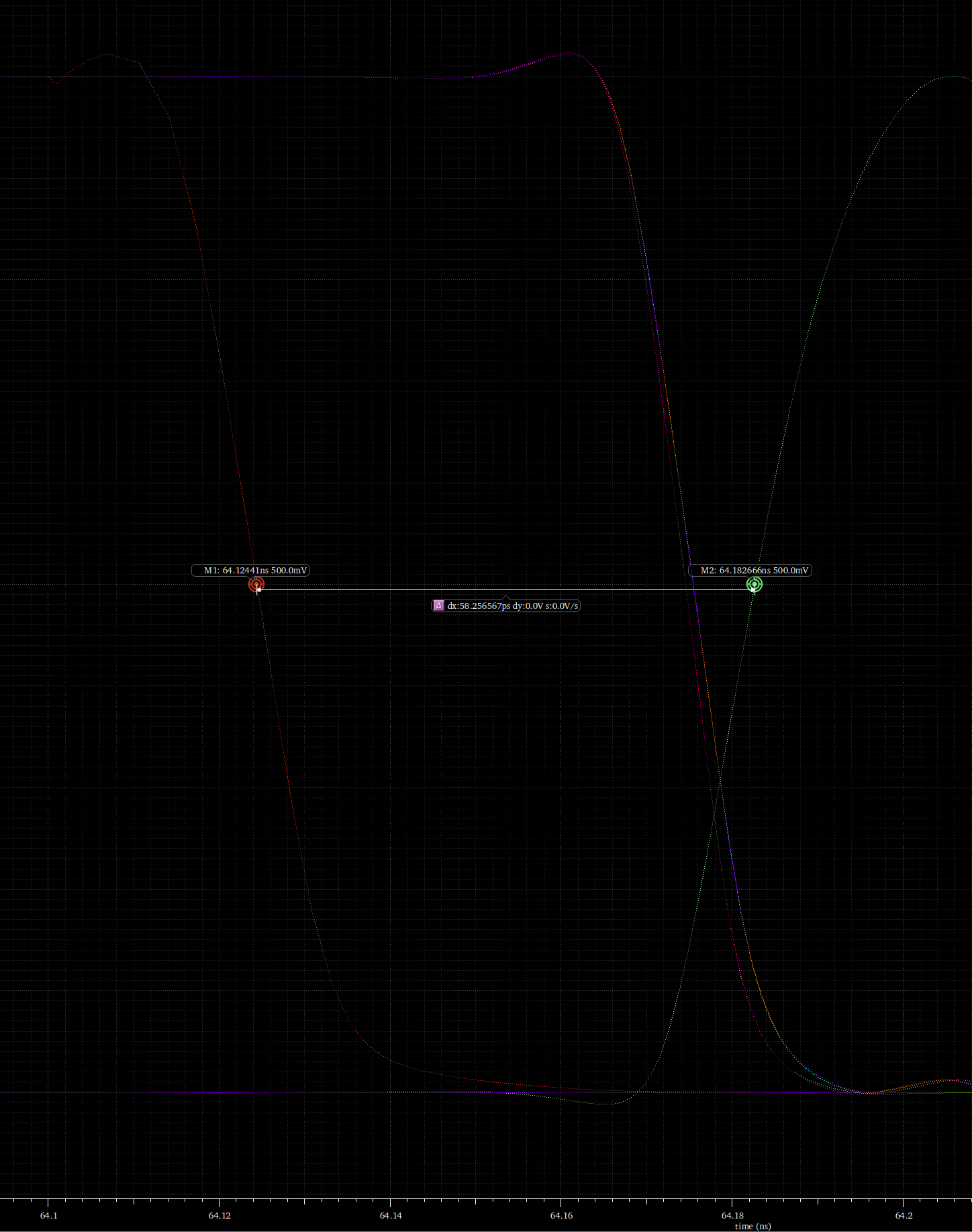
I did some optimization for counter used. Initially we considered using a ripple counter which would have needed less circuitry compared to one using adders. The downside of the ripple counter was that it took longer to update since the clock was passed through each flipflop sequentially, whereas the adder-based timer had the flipflops all clock in parallel.
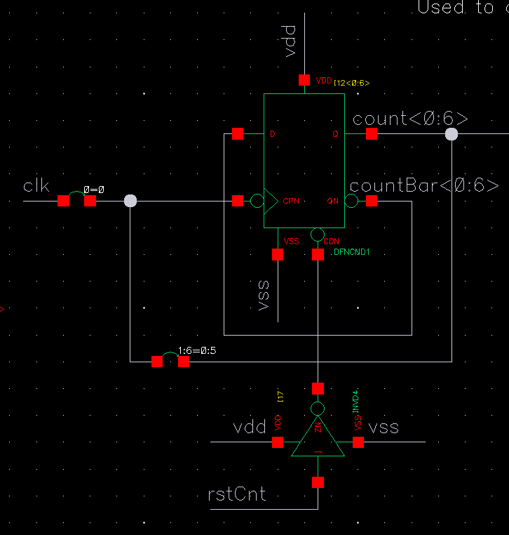
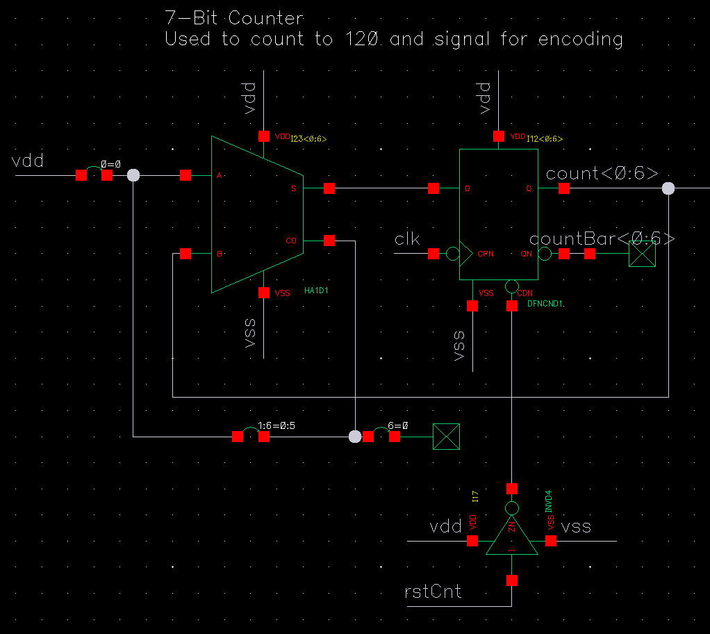
After some simulations the difference in settling time was quite notable, with the adder-based system settling in under 60 ps while the ripple counter exceeded 300 ps. Given that these would be responsible for directing the clock elsewhere in the system it was imperative they operated quickly, so we opted for the adder-based counters in our final design.
Flow Control
I designed these blocks to prevent data flow issues. They would count the number of clock cycles on the input and output and raise flags when there was no remaining space or no more data available. These signals would be passed on to the core.
In addition, it would clock the parallel data into and out of the encoder block when enough data was present and the encoding was complete respectively. Since the encoder was all conditional, a delay was used that exceeded the slowest logic (critical) path to pass a clock pulse on to the output buffer flipflop bank that feed the the parallel to serial flipflop array.

Preparing the logic for this was where I probably spent 60% of my design efforts.
Encoder
I didn’t contribute to the design of this module, it was entirely the work of my partner. Unlike the rest of our logic circuitry that was designed by hand, this was going to be synthesized from a hardware description language file he prepared Verilog. He wrote all the logic out and verified it worked, and then we used Cadence’s tools to generate the circuitry from what was available in the parts library.
Unlike all other blocks in the system, this one was entirely combinational logic, with no clocking.
It was quite a cool process to witness and then to look at the insane web of logic it had spun from his Verilog file.
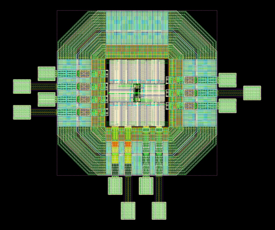
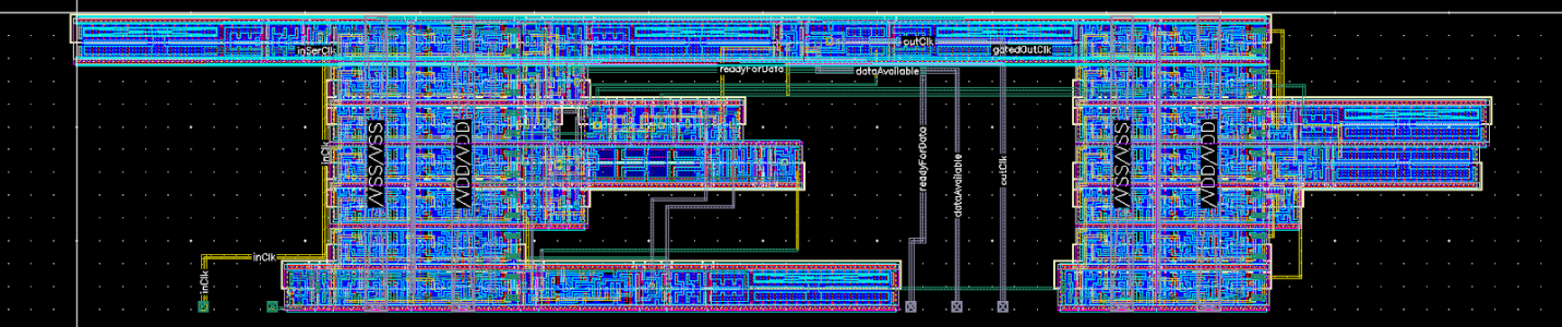
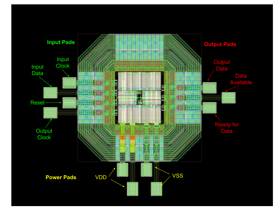
Core and Padframe
The core and the padframe was where the entire design came together, my partner mostly handled this. The difference between the two is that the core was all our logic and circuitry as a unit, the padframe was the ring of pads that encircled the core and would connect our core to the package if this were being turned into a real chip.
As such the schematic of the core and padframe are essentially one and the same.

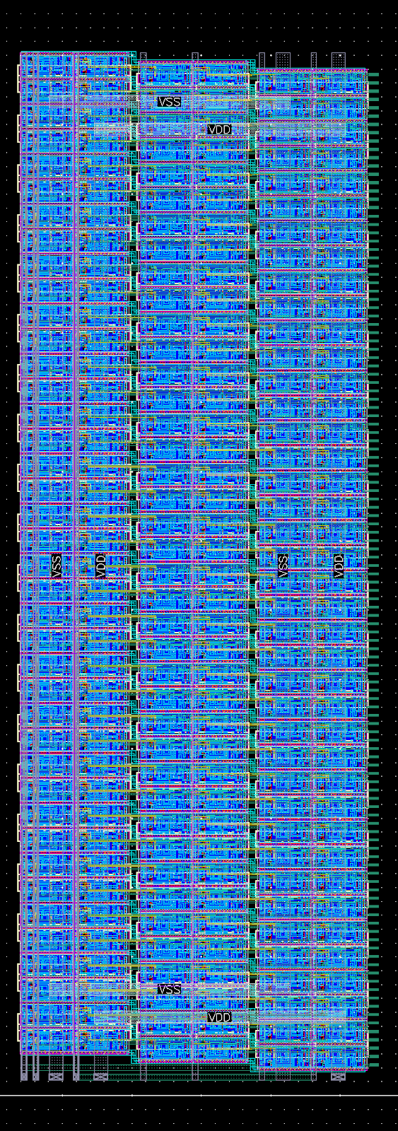
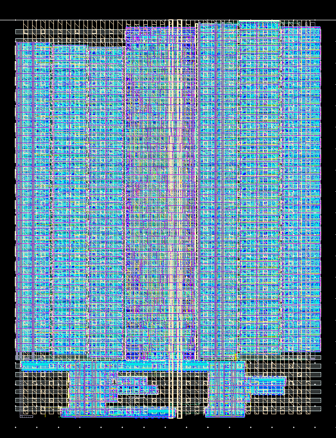
Layout
The layout of our integrated circuit was largely done by hand, the only exception being the encoder logic block. Just like with the circuit, this was done by first laying up the lowest-level blocks and then gradually combining them into the larger blocks. My focus was on laying out the encoder block, while my partner did most of the work on the core and pad frame.
At the start we realized that the majority of the layout area would be occupied by the encoder blocks so I tried to keep them compact and roughly square so that we could later pack them efficiently on the final die layout.
Shift Registers
I began with the shift registers needed for each encoder block. When my partner synthesized the encoder logic block we agreed to have a pitch of 0.6 um for the input/output lines, which was a nice 1/3 of the 1.8 um pitch used for the standard cells. Thus I would have three staggered banks of flipflops on each side of the encoder block.
To accommodate this staggering the routing had lots of zigs and zags, but luckily it fell into a regular pattern so t could be replicated into an array as needed.
Since there were 120 lines into the encoder it divided into a nice even 40 levels to each of the three banks. Unfortunately 128 is not divisible by three so that didn’t come out as pretty.
Flow Control
Laying out the flow control was almost as difficult as deriving the logic for it. This difficulty came from trying to determine how to arrange the blocks since a good portion of the logic went in a single path and could be essentially laid in a line of cells.
In the end I broke it into parts and folded it up to achieve a more square layout that fit nicely under the shift register and encoder sandwich like in the block diagram. This resulted in the logic flowing both left to right, and right to left.
I think I did a good job considering the web of logic, although the gaps probably could have be minimized with a bit more effort.
Overall Integration
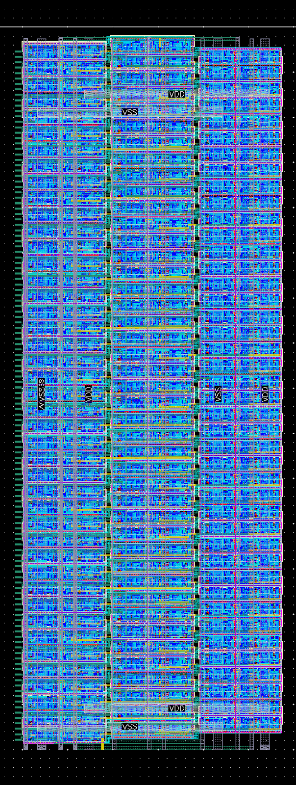
Putting it all together to form an encoder block resulted in a nice squarish block. I overlaid it with a net for VSS and VDD distribution and ran out the signals that would connect further into the core along the bottom.
My partner took these and arranged the eight we needed in a ring with the other core logic in the middle. By placing the logic and multiplexers in the centre and distributing the signals out from there to each of the encoder block, we minimized the phase delay difference between different encoder blocks. The core layout was approximately 240 um by 260 um.
We were pleasantly surprized with how well everything fit together without wasting much space on the die. My partner then placed the core into the padframe he designed, and we got to witness our final design!
Final Results
Prior to laying out our designs we ran some simulations to see how our design would be expected to perform. The results were promising, we could operate at 3 GHz (three times our goal) and our power consumption was about what we sought at 1 GHz, but exceeded 5 mW a fair bit at 3 GHz with an estimated consumption of almost 13 mW.
With the layout completed we measured the final dimensions of the entire layout including the padframe which came out to approximately 960 um by 812 um, which satisfied our 1 mm by 1 mm goal.
When delivering our final presentation and revealing our final layout, our professor who asked us to return to our reveal slide once we finished our presentation to “marvel” at it some more.
-
IEEE 802.3bs Task Force, “Objectives”, IEEE, Mar 2014. [Online]. Available: http://www.ieee802.org/3/bs/Objectives_14_0320.pdf. ↩︎
-
Wikipedia, “Hamming(7,4)”, Wikipedia, June 2023. [Online]. Available: https://en.wikipedia.org/wiki/Hamming(7,4). ↩︎
-
M. Isaka and M. Fossorier, “High-rate serially concatenated coding with extended Hamming codes,” in IEEE Communications Letters, vol. 9, no. 2, pp. 160-162, Feb. 2005. ↩︎
-
Proposal for a specific (128,120) extended inner Hamming Code with lower power and lower latency soft Chase decoding than textbook codes, IEEE Standard 802.3df, Oct. 2022. ↩︎
-
G. Caire, G. Taricco and E. Biglieri, “Bit-interleaved coded modulation,” in IEEE Transactions on Information Theory, vol. 44, no. 3, pp. 927-946, May 1998, doi:10.1109/18.669123 ↩︎