T3.2 PCB and T7 Drivers
Table of Contents
Overview
As part of my master’s I had the opportunity to do a project for course credits, which I decided to do so I could sharpen my practical skills some more than what I would have, had I had just done courses. The project I got accepted to do was to make the circuit board that would host an experimental new coded-exposure image sensor the Intelligent Sensory Microsystem Laboratory (ISML) had produced.
The sensor I was going to work on was their T3.2 sensor, their newest iteration of a Time of Flight (ToF) imaging sensor to determine the distance of objects in a scene from the camera. This was to be achieved through a combination of controlled illumination, galvo mirrors, and specialized pixel design on the sensor. In addition to the hardware design of the circuit board, I was also tasked with preparing the driver code that would run on the embedded Field Programmable Gate Array (FPGA) and allow users to get the readings from the image sensor to them be processed on a host computer.
Alongside the development of T3.2, I also aided in the development of the T7 image sensor system, the highest resolution image sensor ISML had manufactured to date. My contributions to T7 focused on improving the high-speed performance of the sensor in burst imaging and sub-frame readout applications (explained later, trust me!)
Requirements
The project as initially outlined to me had three main deliverables:
- The schematic and PCB design of a carrier board for the FPGA and T3.2 chip
- FPGA drivers to pull data off T3.2
- Improvements to PC drivers for data and driving the galvo system
Overtime this shifted a bit as did the priorities of the lab and the changing situation of T3.2 to reflect this by the end of my project. As shown, my work became more focused on the digital design of the system and moving data around:
- The schematic and PCB design of a carrier board for the FPGA and T3.2 chip
- FPGA drivers to pull data off T3.2
- Lead sub-frame readout of T7
- Improve USB transfer speeds for all systems
- Experiments on T7 for ISSCC publication
Objectives
The primary objective of this work was to get it working with minimal changes to the existing system. This gave me some physical constraints for the the final size of the circuit board and the placement of some parts, namely the image sensor and FPGA. Outside that, I had essentially free reign on how I got things working for T3.2 although it made sense for me to make use of their existing work.
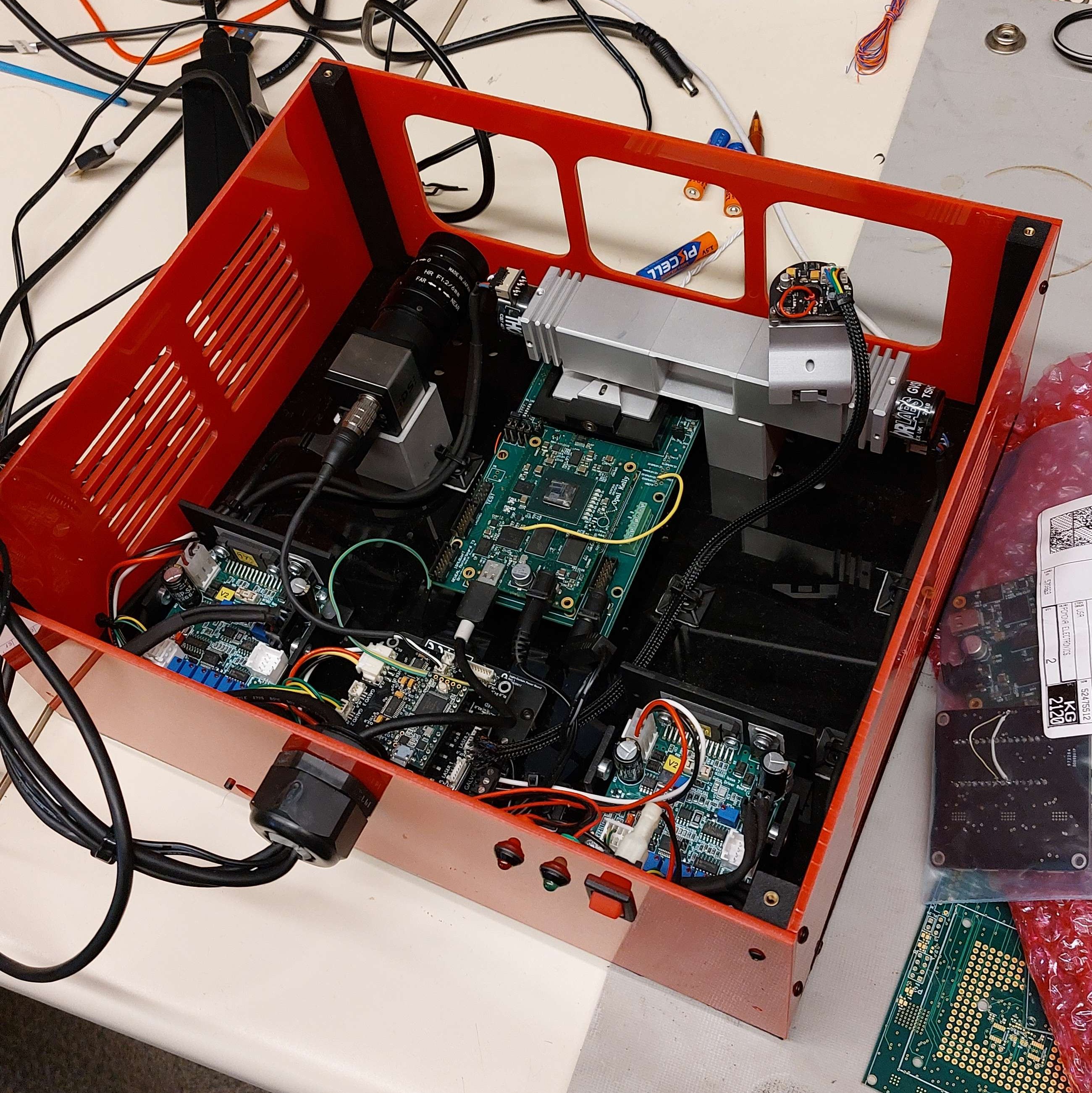
Outside of the T3.2 system, one of my main objectives was to try and get our USB data communication rates up to almost 80 Mb/s, about an order of magnitude above the rate at the start, yet only a quarter of the advertized and verified speed possible by the FPGA of 300 Mb/s.
Takeaways
Ultimately I completed the design and bring up of the PCB largely by myself, based on the work done for the previous iterations leading up to T3.2. I did have the aid of some summer students I oversaw for the programming when it came to those tasks. Unfortunately when we finally inserted the chip we found that the chip failed to function as it was meant to ultimately killing my project so I pivoted to aid more in T7. In the conclusion of my report I prepared for the group, I listed a series of improvements to consider both for the future of the T3 line, as well as things I noticed would benefit all future ISML work.
I learned a lot about designing multi-layered circuit boards, imaging sensors, digital design, and what bringing up a custom chip is like - all things I am thankful to have gained. Some key points for me were:
- The importance of adding pull-up/-down resistors where needed
- Performing power and efficiency calculations are helpful when planning a circuit
- The importance of a well maintained and buffered data pipeline between FPGA and DRAM
- Timing closure importance and the odd bugs that can occur when a system fails to stay in sync
Detailed Report
At the conclusion of the project I submitted a report, which is the basis of this write up. Some parts were modificatied in both content and formatting to suit my website. Unfortunately, since this was a project derived from and ultimately belonging to ISML, I don’t have the right to lay out all the details as I would generally for the other work I post about.
If you would like to read my report in all it’s LaTeX-formatted glory and extended detail, feel free to give it a read by downloading it here.
Introduction
There are a few technical concepts that I will explain to set the stage for the rest of the report regarding the nature of the sensors and systems I was developing.
Coded Exposure Imaging
The functional basics of the cameras developed by ISML is Coded Exposure Imaging (CEI), a modern class of digital cameras. Their defining improvement over traditional digital imaging sensor is per-pixel control of exposure (“coding” or “masking” the image). This is generally done as a series of “subframes” which the resulting cumulative exposure is the frame. This enables different regions of the same sensor to capture light for different periods, which in conjunction with proper post-processing enables novel imaging techniques with applications in High Dynamic Range (HDR), medical, and control system imaging.
At ISML the CEI sensors being developed are multi-tap CEI pixels. Each pixel has multiple taps which are “exposed” based on the masking applied to the pixel array, thus masking pixels does not lead to light being lost, merely “sorted” into different taps during the exposure period. The T3 line of sensors has four-tap pixels while the T7 sensor has a two-tap pixel structure.
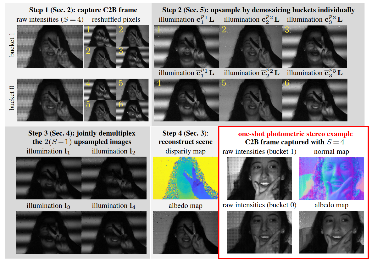
Augmenting these sensors with controlled illumination sources that are synchronized to the coding further enhances their utility, allowing for advanced data to be collected visually often at video rates of 30 frames per second or more. An example of this is demonstrated where a CEI sensor with controlled illumination was able to determine both the normals and albedo (reflectivity) of all the surfaces in the scene.
Time of Flight Sensing
Time of Flight (ToF) sensing is the process of determining an object’s distance by timing the duration is takes for some waves to reflect off an object and return to a source, hence “time of flight”. Sound is often used for this (e.g. echolocation for bats), but light can also be used with the correct sensing system. Light can offer a much finer resolution of depth sensing in a scene, with the trade off being a more complicated system is needed to resolve the sub-nanosecond timing for the speed of light.
The method employed by the T3.2 system is “pulse-based” ToF. Using four buckets which are each exposed 90 degrees out of phase with one another, one can both accurately estimate the ToF given the relative amount of exposure between these buckets, as shown below.
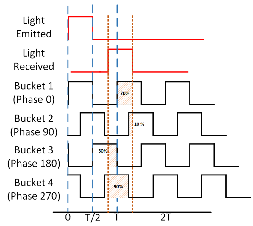
Another benefit of using four buckets is that it allows for the ambient light levels to be determined on the fly and accounted for when calculating the ToF by correlating the different pairs 180 degrees apart.
T3.2 and T7 Image Sensors
As mentioned before, T3.2 is a four tap pixel image sensor, with a resolution of 1032 by 44 pixels. It’s focus was ToF imaging with the capability to do CEI. Due to it being a line sensor it is dependant on an opto-mechanical assembly including of galvo mirrors to redirect light so it may properly scan a scene from top to bottom. Due to issues with the internal Analog to Digital Convertors (ADCs) of T3 used to determine the exposure of pixels, T3.2 was designed with 18 analog outputs for external ADC to perform this duty as a contingency if the issue reoccured.
T7 is a two-tap pixel image sensor, with a resolution of 480 by 640, the highest from ISML to that point. Its primary focus is CEI, with it’s large resolution it has been a good candidate for many new techniques. Since it is a more conventional “square” image sensor, it depends on a simple optical lens to properly focus the scene before it.
Circuit Board for T3.2
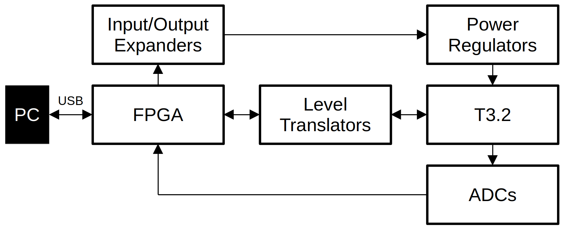
The bulk of my work for my master’s project was related to the design and validation of this PCB. I will try to stay high level here, leaving the details in my report. In short the PCB had to carry all the supporting electronics needed to have T3.2 operate, and then route the signals from T3.2 into the FPGA to then pass onto the host computer, below is a simple block diagram of the system.
There was a draft design made for T3.2 in ISML before I was brought onto the project, which was used as the basis for my design. Furthermore, improvements made to the other host boards in the lab since T3 (namely T6’s and T7’s) were incorporated into the design.
Objectives and Constraints
The major change for the host board from T3 to T3.2 was the inclusion of “off-chip” ADCs to serve as backups in the event the ADCs in the T3.2 chip (“on-chip” ADCs) failed to operate. The remainder of the objectives aligned largely to the original ones for T3. Listed in no particular order, the design objectives for this were:
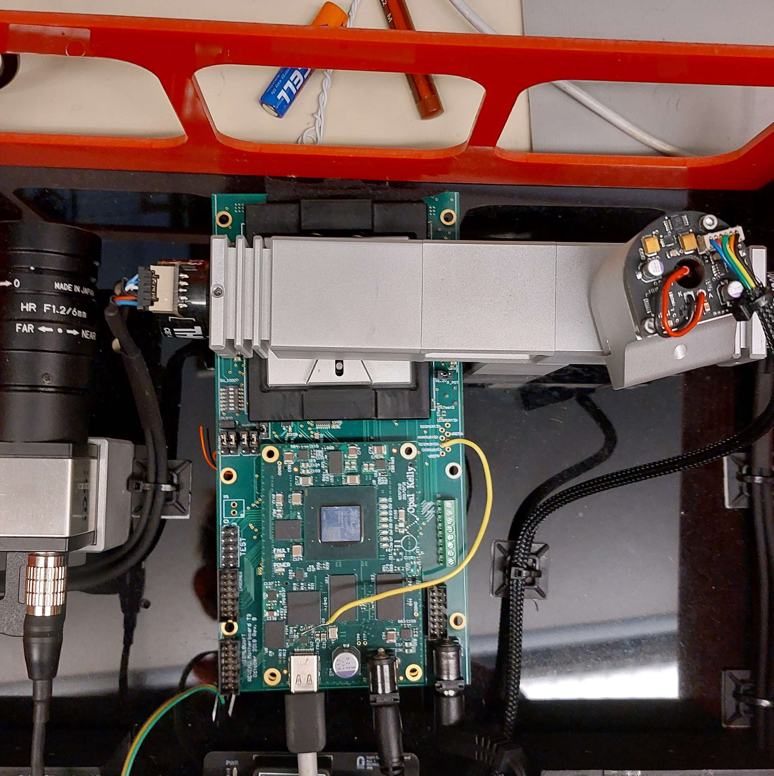
- The new PCB had to fit within the existing enclosure and optical system for T3
- Location of the T3.2 sensor must fall under the current optical assembly (metallic structure in Figures of the system)
- The board was not to interfere with the vertical support to the upper left portion of the host board location and reference camera stand on the left
- The resulting allowed dimensions were 110 mm wide, 170 mm long; with the center of the T3.2 chip placed approximately 40 mm in from both the top and right edges
- The PCB was limited to six copper layers, but could have components placed on both sides
- Handle all the FPGA-sensor connections with minimal delays and phase skew on data buses
- Host the newly introduced off-chip ADCs
- Allow for the digital adjustment of all the power lines feeding T3.2
- Allow for the insertion of external power on the power lines in the event of design failure or power monitoring is needed
Schematic Design
The schematic for T3.2 was heavily based on what was done for T3, and the previous work ISML had done prior to me joining. Most of my contributions to the schematic design were optimizing and renovating subsystems with either improved designs from other ISML projects, or entirely novel designs for the group. Since the work is not entirely mine, I will not be sharing the complete schematics of the T3.2 PCB like I have with my other projects.
Part Selection
The first task I had in January as I was onbaorded was to review the Bill of Materials, BoM, to identify if any parts in the draft design were unavailable or critically low from our preferred vendor and then replace in the design accordingly. Luckily only two minor parts were out of stock and needed replacing, both were part of the voltage reference subsystem for T3.2’s on-chip ADCs.
The replacements were sourced from the design for T7 which has similar components. One component replacement was almost like-for-like, but the other was a linear voltage regulator with a lower current rating. This decrease on allowable current was accepted by the team and I went about working on the schematic further.
Input and Output
Given that the FPGA needed to not only communicate with T3.2 and its supporting circuits but also the off-chip ADCs, it ran out of pins to directly connect to everything. To address the input/output limitation two methods were employed: firstly for “slow” signals such as chip selects or resets a pair of input/output expander chips were added to the circuit allowing the FPGA to operate up to 32 pins with just two of its own at the expense of some latency and bandwidth due to the inter-chip communication.
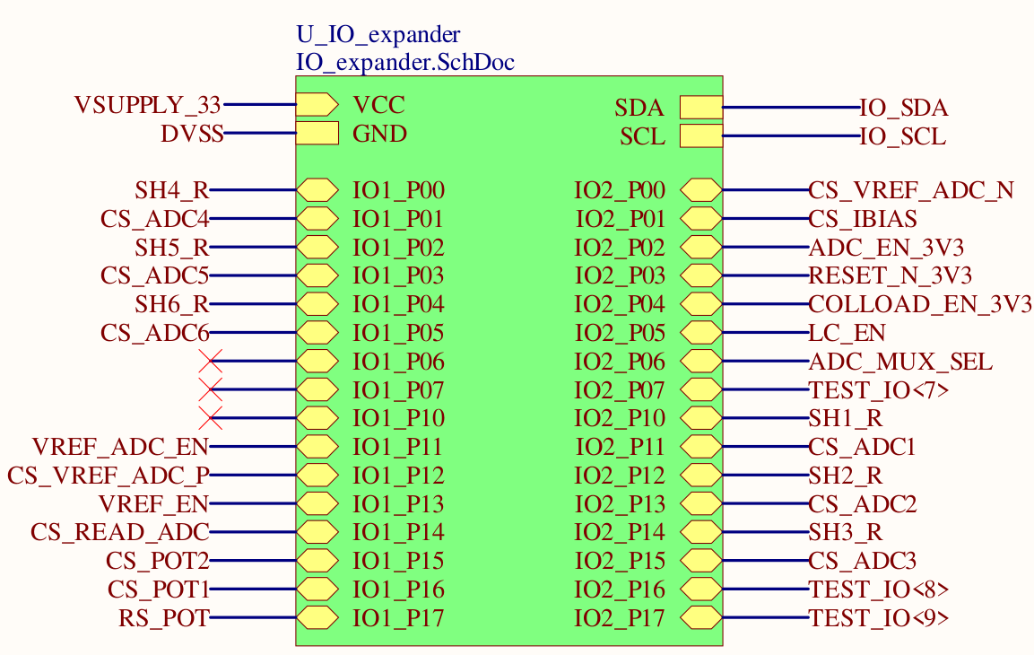
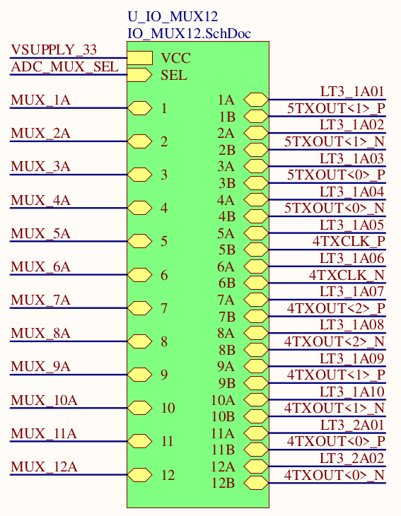
The use of the expansion chips did free up a significant portion of the pins needed for all the “fast” connections to reach the FPGA directly, these lines were the data lines from either the off-chip ADCs or T3.2 itself. Unfortunately the FPGA was still a few pins short, so multiplexers (MUX) were selected to allow the FPGA to switch between sets of signals to connect directly to itself to avoid the latency and bandwidth limitations inherent by the expander chip solution.
The fact that there are essentially two sets of fast signals that are functionally mutually exclusive (off-chip ADCs vs. T3.2 readings) lends to easy multiplexing where the FPGA selects between one entire set of inputs or the other. The design I inherited from the previous student made use of this fact, it had a 48-channel 2:1 multiplexer circuit to accommodate multiplexing the 8 data lines for each of the six off-chip ADCs.

These 48 ADC signals were only being multiplexed with 12 signals from T3.2, so in reality only 12 signals needed to be multiplexed and the remaining 36 could be directly connected to the FPGA. This would reduce the size of the BoM in addition to removing the parasitic effects a multiplexer would impart on connections unnecessarily.
Level Translation
T3.2’s digital domain operates at 1.2 V whereas the FPGA uses 3.3 V signalling so level shifters were needed to translate these signals safely. In addition to the 3.3 V to 1.2 V level shifters, there were a few that worked with 5 V signals needed to operate some of the voltage reference circuitry and others for a handful of 5 V signals from the FPGA to T3.2.
All these level shifters needed to operate at speeds of above 100 MHz to operate effectively, so consideration was put into that when selecting the appropriate chips.
Power Regulators
Eight voltage regulators are needed for T3.2 to be operational in the analog domain: five for the various power rails and three to act as voltage references for the ADCs. All these regulators for T3.2 can all have their output voltages adjusted using the digital potentiometers that form their feedback networks, in addition to being entirely enabled/disabled as desired via the FPGA. This allows for safe start-up procedures to be done automatically and the voltages to be adjust quickly and accurately as desired. These analog supply voltage regulators are all RTQ2520 chips, and are used as per their reference design with minor variations on the feedback topology used.
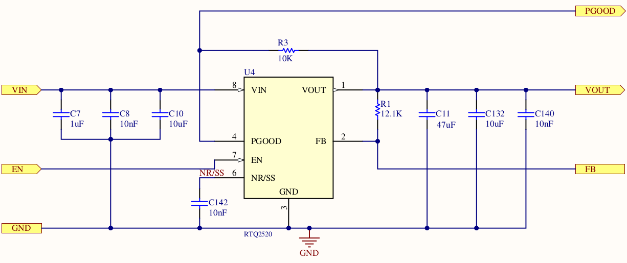
These eight regulators are in addition to the six fixed regulators used to supply digital power to the components on the board. Separate 3.3 V regulators for the FPGA, level shifters, and off-chip ADCs; 1.8 V for the FPGA; and separate 1.2 V regulators for the FPGA and T3.2.
These regulators were all selected based on those used previously for T3 or T7.
Off-Chip Analog to Digital Convertors
The main change in the system design from T3 to T3.2’s board is the introduction of these ADCs. Their purpose being to allow the group to read the analog signals generated by the pixels directly if the on-chip ones fail to meet performance requirements; allowing the pixels to still be used and evaluated on T3.2. 18 analog signals are fed out of T3.2 and must be sampled at rates exceeding 10 MS/s for full utilization of T3.2, so six of the LM98722 Analog Front End chips were used which can sample 3 channels at rates of 15 MS/s each.
Board Design
The majority of my time designing the T3.2 hardware was laying out the custom circuit board since the schematic was largely prepared for me as I mentioned before, but I ended up needing to layout the PCB from scratch to arrange it to fit the new ADCs and their supporting circuitry.
Floorplan
The board was laid out to satisfy the physical requirements imposed on it by the optical assembly it interfaced to. The allowable footprint was 110 by 170 mm, which was completely used. T3.2 had to be placed such that the center of the optical sensor was the required 42 mm from both the top and right edges. The FPGA was placed along the bottom in keeping with ISML design patterns. The remaining systems were then placed based on functionality, for example the level translators and the off-chip ADCs were placed between the FPGA and T3.2 while the voltage regulators were generally placed in proximity to the devices they were intended to supply.
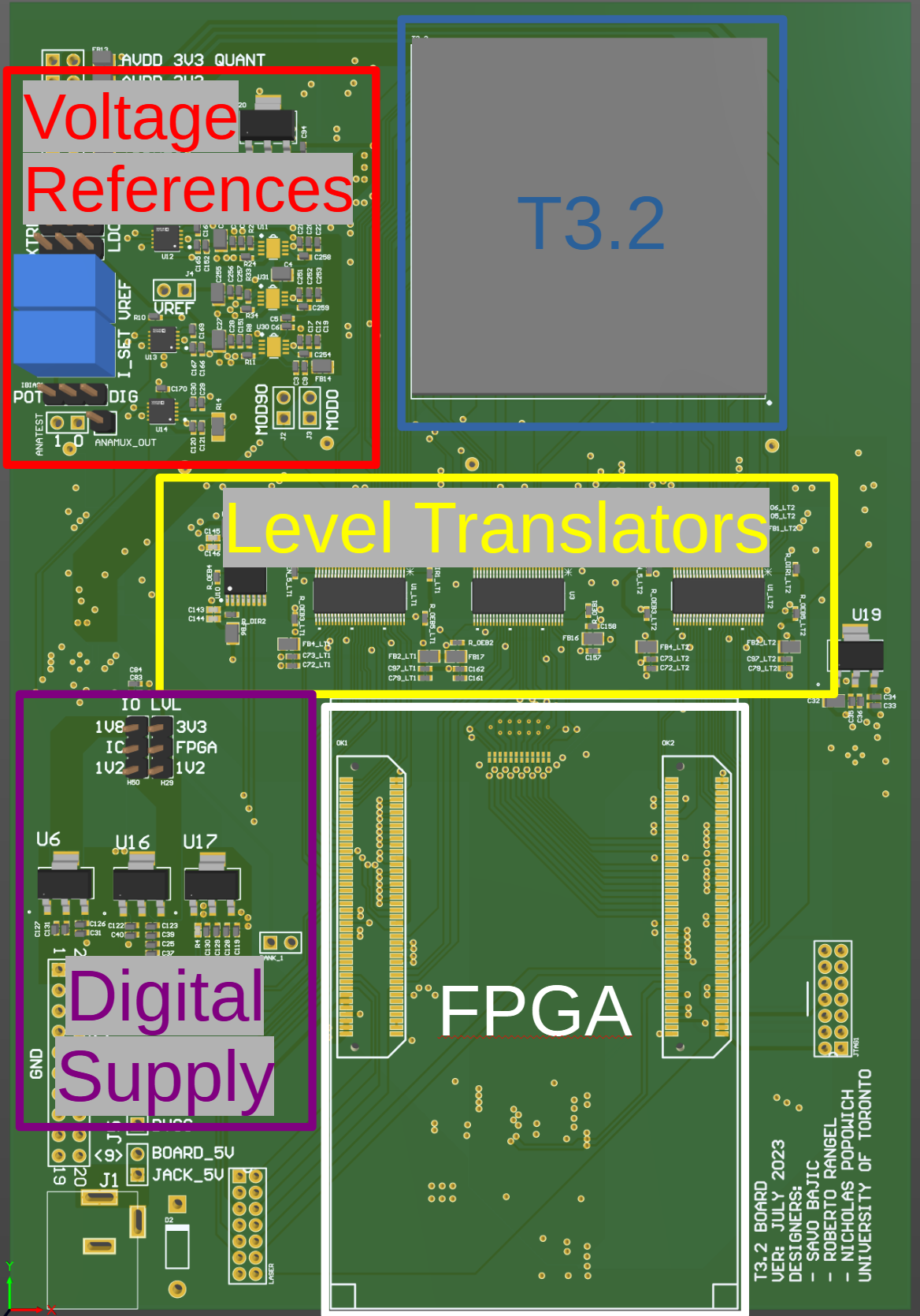
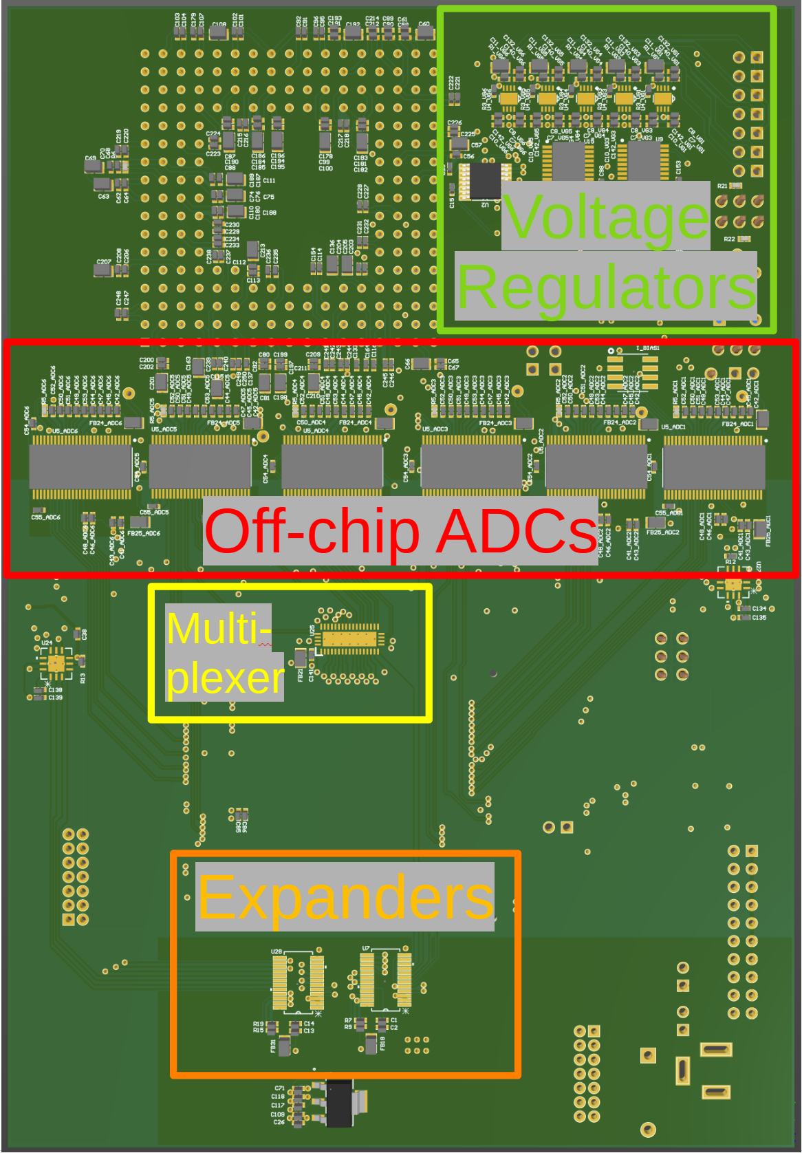
The FPGA, digital level translators, and T3.2 sensor were all placed on the top layer to allow most of their data traces to be run on the top layer alone, omitting the need for vias which would complicate routing and impede signal transmission. To further preemptively improve the routing stage, many of the components on the top were shifted to the right of the board with T3.2 to try and equalize all the signal lengths. Given all the components on the top side of the PCB, the off-chip ADCs would only fit on the bottom face, which was acceptable since they were only meant to be a contingency if the top failed.
The decoupling capacitors needed around T3.2 were placed on the bottom so they could remain close to the pins without impeding the optical assembly going around the sensor on top.
Routing
This was my first time routing a multi-layer board! So that was a fun new thing to try out. The T3.2 board had six (6) layers; the two outermost layers for local component connections, the two inner layers reserved for power pours: one for the separated analog and digital grounds, and the other power layer for the common positive supply rails, and the two innermost layers for long data signal runs.
The most important data traces on the board would be the data buses between the FPGA and T3.2, specifically the mask stream into T3.2 and the digital output from it. To ensure that these signals were minimally degraded the traces were kept to the top layer for the majority of their runs except when passed to the multiplexer which was mounted to the bottom. This led to an iterative process of reassigning connections to the FPGA, multiplexer, and level translators to prevent any trances needing to cross over one another.
Once these main connections were formed, other relatively high speed and fan-out buses like the SPI bus used for interacting with many of the supporting circuits were laid out. Eventually progressing to slower and less critical traces which could be more windy. The final result of the data routing is demonstrated below.
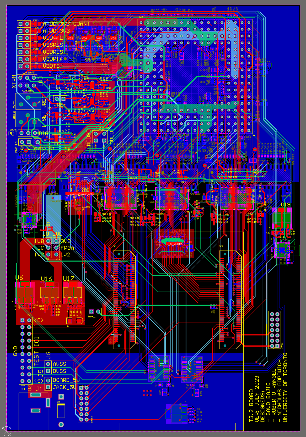
An unfortunate side-effect of having all the high speed buses on a single layer with long parallel trace lengths as shown is the increased cross-coupling between the individual traces which may introduce glitches as the data rate is increased.
One important metric that was verified in reference to the high speed buses prior to committing the board to production was the bus skew. This is the relative delay between the fastest and slowest trace that belongs to a bus based on the speed of electric signals and the trace lengths of each individual signal in a bus. If this is allowed to get too large then the signals may arrive across different clock cycles at the destination and be misinterpreted. Observing the results the maximum skew across both buses was approximately 150 ps which was determined to be negligible due to this representing about 3 % of the 5 ns clocking period to be used.
Looking back on my time routing, one feature I liked in Altium that isn’t built into KiCad is their “room” feature where you can replicate the layout of different sub-circuits in the PCB based on the hierarchy of the schematics. I made use of this with the voltage regulators and references which were repeated circuits. This saved me time since I could focus on designing one system excellently, and then just copying it multiple times.
Production and Validation
Since this board had a few hundred components - many of which were fine pitched, the boards were not assembled entirely by me or anyone else at ISML: instead the design files were sent to a contract manufacturer to handle the majority of assembly, and we would add the final touches that we could confidently do by hand to minimize costs. This way we could safely assume that the PCBs were correctly assembled when we received them, all we had to ensure was the correct installation of many through hole headers and potentiometers.
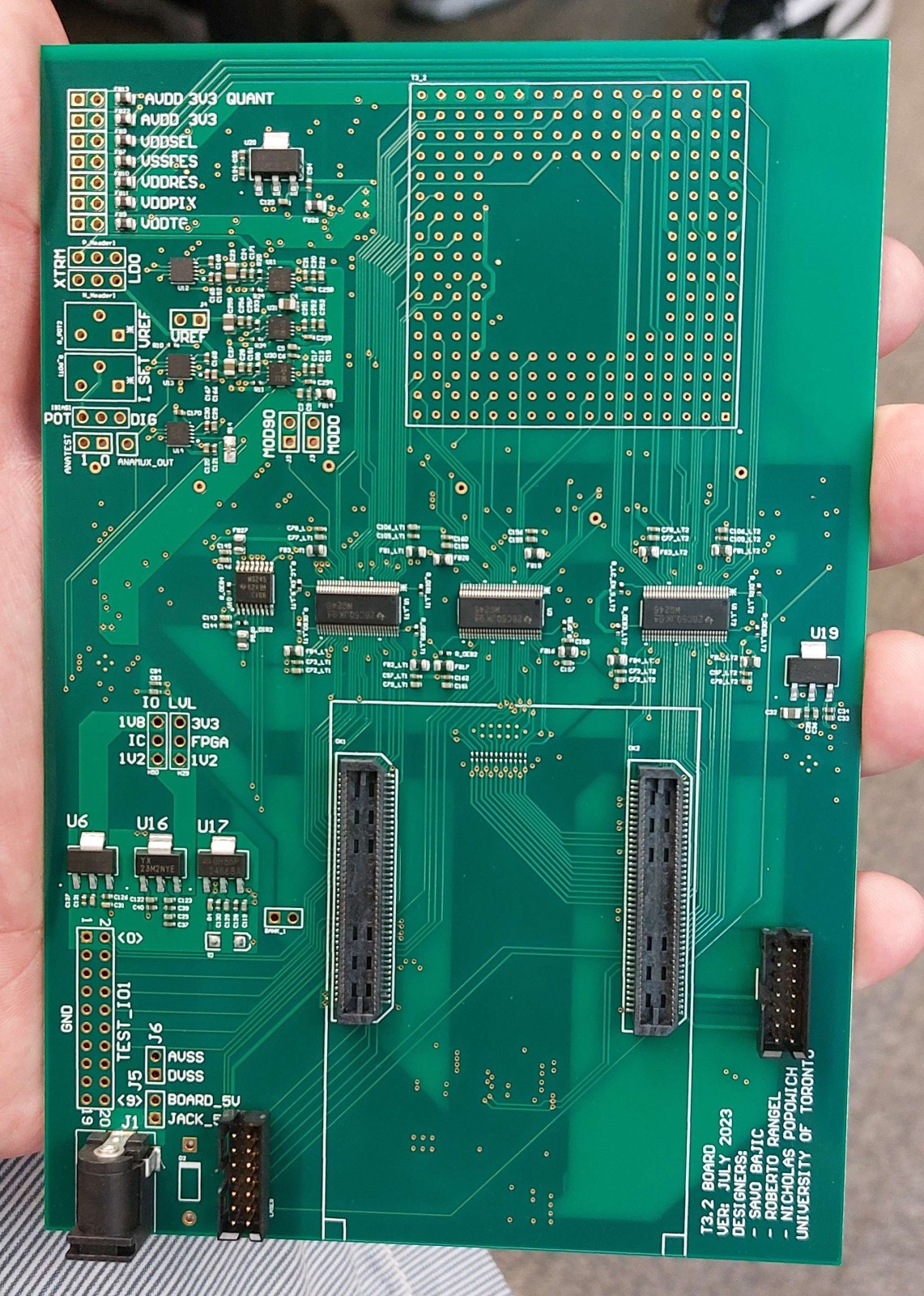
After the assembly was completed but prior to the installation of any T3.2 sensors - of which only exist a couple dozen, I had outlined a few simple tests to verify the boards were ready.
- “Smoke Test” - Apply power and monitor board to ensure none of the components are getting
excessively hot
- Off-chip ADCs and their voltage regulator were found to heat up quickly when power was applied
- Remedied by disconnecting the ADCs from power. This was acceptable since they could be reconnected later if T3.2’s internal ADCs were found inadequate.
- No other parts were found to heat up when power was applied
- Voltage rail verification - Inspect all voltage regulators to be outputting the expected values
- All fixed regulators met their expected outputs
- Varying regulators met their expected default outputs based on the power-on settings of their potentiometers and feedback circuitry
- Data path verification - Checking continuity between critical points
- All critical data paths (e.g. DIGOUT, MSTREAM) met expected connections leading to the seat for T3.2
- NOTE: This test is generally performed by automated testing equipment at the end of PCB manufacture by vendors to ensure the produced boards meet specification prior to the installation of any parts. This test was performed to check that solder joints (especially those done by hand at ISML) were valid.
All the boards passed these tests and were deemed ready for the addition of T3.2 chips, however they were not installed at this point since I wanted to develop the drivers for the PCB prior to adding a T3.2 chip to prevent accidental damage as the drivers were developed.
Drivers for the T3.2 board
With the boards properly assembled I moved to preparing the supporting code to get T3.2 operation and outputting the image data it was meant to. First I needed to get the peripheral circuitry up and running so that the board could properly host T3.2 once it was installed on the circuit board, without fearing it may damage the chip.
The majority of the driver code I developed was written in Verilog for the embedded FPGA, with some Python code prepared for the host computer. Some components of the drivers were adapted from other ISML work namely T7 and previous work for T3.
Peripheral Circuity
I use the term peripheral circuitry to encompass anything on the board other than the FPGA or T3.2, which is in summary:
- [General purpose] Input/Output (GPIO) expanders
- Level translators
- Signal multiplexers
- Off-chip ADCs
- Digital potentiometers
- Voltage regulators/references
The majority of the peripheral circuitry uses Serial Peripheral Interface (SPI) to communicate with the FPGA, making an SPI driver for the board a requirement. As part of this protocol the chips must receive a “chip select” signal which is when a dedicated pin on said chip is pulled low, all of these chip select lines were moved from connecting directly to the FPGA for T3 to the input/output expander chips for the T3.2 board. These expanders are controlled by the FPGA using a second protocol: Inter-Integrated Circuit (I2C), which in turn necessitated its driver on the FPGA.
GPIO Expanders
Since all (other) peripheral circuitry depended on the correct operation of the input/output expanders to enable or select the appropriate chips, this was the first driver developed. It was composed of two parts, an I2C interface for the FPGA pins, and a wrapper module which would read in the desired state for the expanders’ pins and convert that into commands for the I2C driver to enact. Due to I2C only being used for the expander chips, it was fine to abstract it away like this, rather than have some central I2C driver from multiple drivers to utilize.

A benefit of this approach is that should there be a future revision of the T3.2 board (perhaps for a T3.3 sensor!) where off-chip ADCs are no longer needed freeing up FPGA pins, the expander driver can be removed entirely and the connections that were previously made to it can be routed to FPGA pins directly.
The actual behaviour of each module was also relatively simple owing to the division of function. The I2C interface module simply idles waiting for a command, then it will assert that it is busy as it executes the command, before returning to idle until its next command is received. The commands follow a simple format: 7-bit address (for the expander chip), 8-bit target register address on the expander, 16-bits data to write to register, all padded with a leading zero to make it 32 bits wide.
The wrapper idles by monitoring the pin states it is supplied to the last set it enacted via the interface, when there is a change between clock cycles it reacts by asserting the busy flag and generating the required command for the interface module. It then waits until the interface completes the transaction before deasserting its own busy flag and returning to idle.
The busy flag is very important for ensuring that the correct sequencing can occur in the system. If the FPGA had the connections done directly to pins, code in the FPGA can safely assume that by the next clock cycle that pin is in the expected state. However with the expander chips this assumption is far from the truth since the I2C transaction takes approximately 90 microseconds to complete, 9000 clock cycles at the 100 MHz the FPGA generally operates at. So for modules that need to be sure that the pin is in a desired state before progressing (e.g. an SPI driver selecting a chip), it can monitor the state of the busy flag to know when the pin has reached the desired state.
After some testing and tuning to increase the communication speed to the maximum supported by the input/output expanders the driver was complete and latency was measured to be the aforementioned 90 microseconds. With this working the level translators, multiplexer, potentiometers, and voltage regulators could all be enabled and/or selected.
SPI System
The SPI driver was based off the design from T7, modified to work with the input/output expander via the I2C driver for chip selection. Unlike the I2C driver which receives commands from a wrapper and is thus “hidden” from the user, the SPI driver is configured on the FPGA to receive instructions directly from the user (or rather our host-side driver software) using the OpalKelly FrontPanel system. These instructions contain both the target device address as well as the information to transfer.
The modification needed to adapt T7’s driver to T3.2 was to add additional states internally to respect the time it takes the I2C/expander driver to toggle the chip select pins as needed. This was done by monitoring its busy state to ensure that it was asserted following a requested change in the chip select pins and then advancing to next state once “busy” was eventually deasserted following a completed pin configuration. The resulting system is shown below.
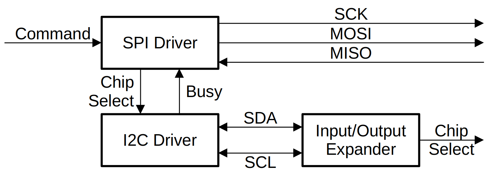
One limitation of the driver presently employed on T3.2 is that it does not record the data it is provided during the transaction from chips, it merely serves to command other chips. This is implied in the block diagram.
Voltage Regulator Drivers
The voltage regulators controlled using a combination of both the input/output expander and the SPI drivers. The voltage regulators used only received signals to enable or disable them directly (via the expander), their output levels were indirectly controlled by adjusting the settings of the digital potentiometers placed in their feedback networks.
The driver for these made use of the existing SPI driver interface, so no Verilog code was prepared for this to work on the FPGA, it was all developed as part of the Python driver for the T3.2 camera. It took the form of a function which received a target channel and the desired voltage to set it to. It would then derive the required SPI command needed for that given voltage channel to approximate the voltage based on the analytical model of the feedback circuit and push it through the SPI pipeline.
This worked for the analog domain power supplies, however the potentiometer used for the analog reference voltages failed to respond as expected to the instructions. I believe this has to do with the SPI protocol configuration and the driver not being designed to handle different phase (“PHA”) chips. This minor issue with the references led to them simply being bypassed and shorted to their respective extremes to allow development to continue for other parts of T3.2.
Off-chip ADC Drivers
There was no development of drivers for the off-chip ADCs. This was skipped so efforts could be focused on getting T3.2 operational as originally envisioned using its internal ADCs - only returning to work with these off-chip ADCs if it was deemed necessary.
T3.2 Interfacing
With the board’s circuitry and peripheral drivers deemed functional and safe, a T3.2 sensor was installed so that driver code for it could be developed. This step was not as smooth as we hoped for as we accidentally misaligned the sensor a couple of times before finding the correct alignment, likely damaging the affected sensors. The issue came down to two causes: the packaging marking on T3.2 not being pin 1’s corner, and the packaging for the T3.2 sensor had some additional but unused pins on the interior meaning it would fit the seat in a few different orientations without mechanical issues. Once T3.2 was properly seated, the work began on getting T3.2 operational with the right code.
With T3.2 largely resembling T3 in terms of their digital system, the hope was that minimal modifications would be needed to port the existing code base for T3 to work with T3.2.
The plan for developing and verifying T3.2 was to start at the bottom of the data flow as shown below, configuring the sensor and gradually working up through the other stages to be certain that there were no unexpected issues between the stage being worked on and the FPGA.
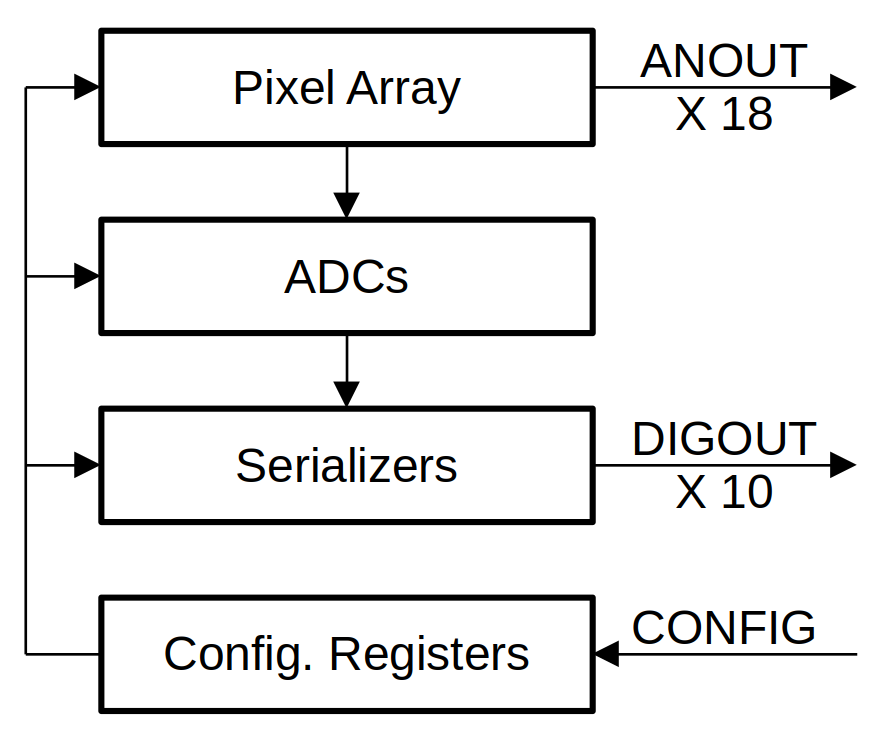
Each step in developing drivers for T3.2 was as much a test of the drivers working as it was a test of T3.2 behaving as designed to, since it had yet to be used by the lab.
Configuring T3.2
The first step in operating the sensor is to configure its control registers to have the sensor work in a given manner. This would allow the sensor to be set into its various test modes which would allow the driver for T3.2 to be gradually developed knowing the expected behaviour of the sensor in these test modes. Due to some of the internal differences relating to the analog systems in T3.2 from T3, the control registers were different so a new driver needed to be prepared.
Configuration is accomplished using a serial interface, not unlike SPI, where data is shifted in bit by bit. However, there is no chip select nor a constant output pin for the stream from T3.2. Instead there is a signal to load in the deserialized data stream and an output pin can be enabled by writing to the right configuration register. Due to the similarities of this protocol to SPI, its driver was used as the basis for this with modifications made to pulse the data load signal at the end of transmission.
To verify if the configuration was operating correctly, the test configuration stream used was intended to connect one of the test outputs to the output of the configuration shift register. Thus if the system was working correctly then the output would return the previous command register setting as the new one was clocked in.
It took some time but there were two issues with the original T3 driver that I rectified and with help of others resulting in a working configuration driver. Firstly, we were originally looking for a response from the wrong output pin on T3.2 so it was not possible to verify the response. Secondly, the order of bits fed into T3.2 had to be reversed to properly enact configurations.
Reading the Serializers
The first stage in reading actual image data is to operate the serializers on-chip and then deserialize the data correctly on the FPGA’s end. These were 100 MHz Double Data Rate (DDR) serializers and thus output data on both edges of the clock signal, effectively outputting 200 Mb/s at max speed. The most basic test was to supply a clock to the output stage with test mode enabled for the serializers in the configuration register. The expected result was a repeating 14-bit sequence 11110000110010 on all output channels.
Unfortunately the tests did not achieve this outcome. With test mode supposedly enabled, the digital outputs were all holding high as they were clocked. Other tests were attempted to try and diagnose the issue but none had any meaningful results. The following tests were conducted:
- Clock speed - It was possible that the clock speed was too fast for the serializers or the level translators. It was found when directly probing the clock input to T3.2 it was partially attenuated by the level translator which was operating at its maximum rated speed. Decreasing the clock rate did not help.
- Configuration register - The wrong bit might be set in the configuration register so test mode is not actually enabled. A proposed test is to set the entire control register to all 1’s to guarantee test mode, but this was not been attempted by me.
- Serializer design issue - The serializer design in T3.2 is different to the one used for T3, it could be possible that the design doesn’t function. Simulations in the sensor design software, Cadence, strongly support the design as valid though.
- The chips were faulty - Perhaps there is some damage on the test chips. Shouldn’t affect them all equally though, and they all respond to the configuration streams correctly.
The root cause was not determined as my attention was shifted to helping with T7 for the final weeks of my project period. This is where my driver development for T3.2 paused since it was impossible to assess the on-chip ADCs without functioning serializers.
Work on T7
During the summer as I worked with ISML, I helped on and off with developing T7 - sometimes directly, other times overseeing the work of undergraduate students working for the lab.
Towards the end of my term with ISML, my focus was shifted to aid the team in the ISSCC conference submission. Originally T3.2 was meant to serve as part of it, but given the troubles I had they decided to go all in with T7 and needed my help to develop a few new features for it in time for submission. This work was related to driver and software developments (in Verilog) as they already had a host board prepared for T7 by another student.
Subframe Readout for T7
On T7 there are two operating modes for the on-chip ADCs: normal 12-bit operation, and a 1-bit mode where the ADC is used like a comparator. The reasoning for this is that it can enable Flux to Digital Conversion (FDC) thanks to more frequent frame readouts. Flux to Digital Conversion is an alternative way of measuring the luminosity of a scene where instead of recording the value of each pixel at the end of exposure (essentially taking the integral of light striking it), the time it takes a pixel to cross a threshold is monitored (providing the derivative, or light flux) which is then extrapolated to estimate the true “brightness” values that the pixel would have at the end of exposure even if it might become saturated.
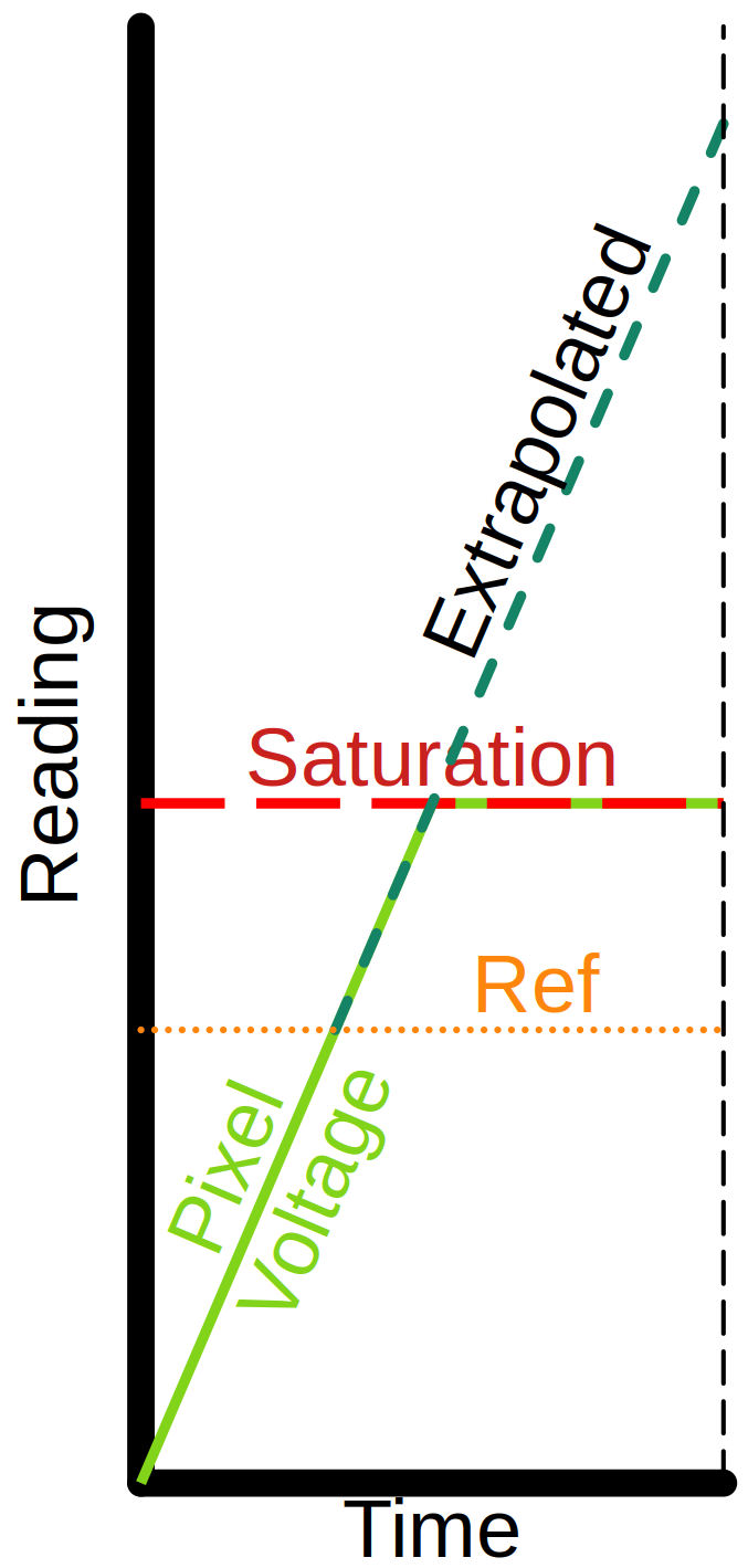
The critical part of this process is the high frequency frame scans, T7 being capable of up to 2000 of these “subframes” a second. The problem with the code that achieved the 2000 subframes a second is that it was not fed live to the host computer, a short period of video was recorded to the Dynamic Random Access Memory (DRAM) on the FPGA and then uploaded to the host in a burst while the camera stops recording (because the DRAM is busy dumping the footage).
BRAM and USB 3.0 vs. DRAM Hypothesis
My goal was to help create a system that could stream the full 2000 subframes a second to a computer live. On paper this was well within the realm of possibility: each 480 by 640 pixel frame at 1-bit of pixel depth would require \(480 ∗ 640 ∗ 1 = 307200\) bits, at 2000 a second that would be just under 615 Mb/s, or 76.8 MB/s. This corresponds to approximately a quarter the verified 300 MB/s bandwidth achieved with the FPGAs employed in the ISML lab.
The proposed idea was simple, remove the DRAM that was preventing the easy streaming of data through the system and replace it with something that can offload the data quickly. This was deemed to be an ideal application of using the onboard Block Random Access Memory (BRAM) of the FPGA and streaming the data at full speed to the USB without storing it for a notable amount of time. As long as the USB 3.0 connection would be able to move data off the FPGA faster than the data was generated (which it seemed to be able to), then the buffers would never overflow and the camera could run at full speed.
There was work done prior to my involvement as I was taking over for an outgoing master’s student. These initial prototypes did eliminate the DRAM component, however they were only able to sustain about 100 subframes a second throughput.
Optimization of Data Streaming
There were two angles to approach hastening the streaming: the host computer’s processing (done in Python) or the FPGA’s code. The Python client was struggling to keep up with displaying the data on screen with all the processing it had to do, but if it was only required to save the data to the drive it, was able to maintain the required throughput when data was available. I looked for ways to improve the system speed by speeding up the existing transfer speeds from the FPGA so more data could be made available to the host and by performing some operations on the FPGA to save processing time on the host.
Speeding up the transfer rate required a few tricks, the main one was the reorganization of how memory was used inside the FPGA. Originally two separate buffers were used to hold the outgoing data to form a bus width of 320 bits since that was the amount of data deserialized per half-row. Changing this to a single narrower, but deeper, buffer that was implemented in BRAM improved the system’s performance and provided some much needed timing slack for the other optimizations I was trying to implement.
I intended to use the pipelining and parallelization of FPGAs to perform some of the common data manipulations that the host computer was performing to reduce the post-processing time for the stream frames. The operations I had a specific interest in performing was re-organizing the order column data was fed into the deserializer to match reality. Unfortunately any attempt to do so that deviated from how it was handled data prior to my involvement led to timing issues the corrupted the readout portion results.
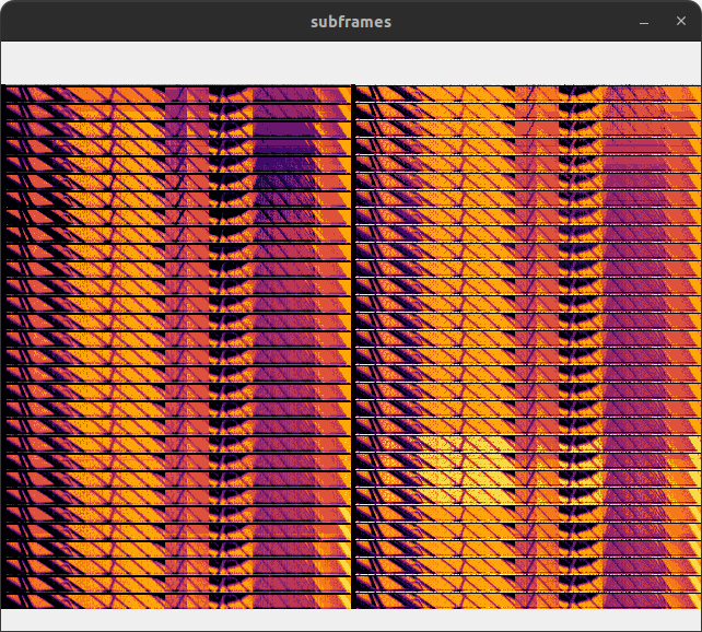
In the end, the sum result of the work done to speed up this system achieved a throughput of approximately 250 subframes a second, which was only about a tenth of what was desired. There was no clear bottleneck in the system at this point.
USB Investigation
Due to the disappointing results from the optimization, I tasked two students to try and replicate the results for the high transfer speeds advertised of the FPGAs - without working in the framework of a camera (so they could just stream dummy generated data). This way one could observe what connection configuration yields the best transfer rate and then gradually build up the camera system around it so as to not disturb the communication setup.
The result of their work was that they were able to both achieve transfer rates of around 300 MB/s as advertised, however this was only feasible if there was no gap in the supplied data. Their results showed that the intermittent generation of frame data combined with limited buffer space available on the FPGA meant that the transfer was constantly starting and then stopping transfers as it consumed all the data. The repeated start/stops adding time overhead to the transfer ultimately limiting the throughput.
The only way forward indicated by this was to have a larger buffer that doesn’t need the transfer to start/stop transferring as frequently, as was the case with the original DRAM system. This however would likely need significant rework of that memory module to make it more streamlined so it can read and write to memory in quick succession.
Generative Masking
Generally the pixel masks for CEI sensors from ISML are generated by the host computer and uploaded to the FPGA pixel-by-pixel and stored in memory on the FPGA for each subframe before uploading the masks to the sensor during exposure.
As part of the lab’s efforts into adaptive masking algorithms with spatially varying burst imaging, I worked on an alternative approach to handling masking. The theory was that as long as the subframe number is known, the size of burst imagining tile a pixel belonged to, and the position (column/row) of the pixel in the array, it can be mathematically determined whether it is needed to be exposed or not, rather than depending on a mask for each of the subframes.
This would allow much less of the memory to be allocated for buffering the mask data since only one “tile size map” would be needed for any number of subframes with a bit depth based on the maximum tile size, rather than buffering several masks worth of pixels. It also allows for the FPGA to easily adjust its masking internally based on some algorithm in the future. By limiting the valid tile sizes to powers of two, the mathematical expression for whether or not a tile should be exposed can be expressed using the following formulas where \(s\) is the subframe number, \(t\) the power of two for the tile size of a given pixel, \(c\) and \(r\) the pixel’s column and row in the image, \(e\) being whether of not to expose that pixel.
$$ a = s \gg t == (c\bmod t + t \times (r \bmod t)) $$$$ b = s \bmod t == 0 $$
$$ e = a \text{&} b $$
In the equations, \(a\) is true when it will be the that pixel’s turn to be exposed within the tile; for example in a 2 by 2 tile, the top right pixel is the second to be exposed. \(b\) is true when the that given tile size is meant to be exposed based on the largest tile size, for example if the tile size for a pixel is 1 but the maximum is 4, then this will only be true every fourth subframe. To implement this tile map parsing logic nicely on an FPGA a series of counters which would rollover at specific values are used in place of modulo operation to reduce logic complexity and ease timing since finding the modulo of something is essentially counting up to that number but restarting a second count periodically. E.g. \(5 \bmod 3 = 2\) which is the same as clocking a counter with a maximum of 2, five times: 1, 2, 0, 1, 2. To select what value to modulo by, one simply selects the counter with the corresponding limit.
This was successfully implemented and tested using Verilog, with a sample result waveform shown below. It was eventually developed so that an arbitrary image size and masking column spacing could be applied and the hardware would handle it.

Although the tile map parsing logic was completed, there was a change in priorities prior to the completion of the tile size map generator, so it is not yet complete. I believe it would not take long to complete the effort if effort was once again dedicated to it.
I believe that this approach could have benefit for other pattern-based, or predictable mask behaviours such as a map to define the number of subframes to expose a pixel for in high dynamic range photography/videography applications, or for regions of interest in slow motion videography.
Conclusion For My Master’s Project
Reflecting on the status of the T3.2 system it was unfortunately far from complete when I finished my term, held up by the issues related to the serializers and an overall lack of time invested into the system due to changing priorities for the Intelligent Sensory Microsystems Laboratory Image Sensor group. I believe that if given more time either a solution to the serializer issue could be found or work could begin on bypassing them entirely using the off-chip ADCs. I am confident that the circuit board I designed is able to support these efforts as it stands.
Regarding my work on T7, I believe that the efforts into subframe readout held value, even if they failed to reach the performance that was desired. They revealed that an effort to revise the DRAM module rather than attempting to eliminate it entirely with BRAM might hold the key needed for maximizing our effective data throughput. I believed generative masking held the most promise for the group immediately following my departure as it heavily related to the group’s focus on burst imaging applications and adaptive masking algorithms at the time.
I wish ISML the best going forward, I hope they can make the progress they aspire to! As part of my report I appended a list of “unfinished business” to help them continue my work.