FPGA Video Processing System
Table of Contents
Overview
For my digital systems class in my masters we had to complete a group project. I teamed up with three others and we choose to do ours on making a video processing pipeline on an Field Programmable Gate Array (FPGA). The FPGA would control a camera, get a video feed from it, apply some process on it, and then display it on a monitor over a VGA interface. The point of using an FPGA in this rather than a computer was that it would be able to do this much more efficiently and with lower latency.
We not only successly accomplished our original intentions, and exceeded our objectives, but actually ended up adding a nifty feature: digit recognition! All accomplished in hardware, without any soft-core or co-processor needed.
My main contribution to the project was the video output stage. Originally I anticipated this to be simple, just read in the pixel values and synchronize it with the screen timings - then I’d be free to contribute to other parts. However, this was far from the case since we needed the output to be broadcast at 60 frames per second (fps) regardless of what rate we were processing video. So implementing the frame buffering system was what really took up my time.
Requirements
- Provide video output at 10 fps
- Use only hardware for video processing
- Apply meaningful video processing (e.g. edge-detection)
Objectives
- Achieve the full 30 fps support by our camera
- Not require any external memory or significant buffers
- Latency below 200 ms
- No pixel glitches visible
Takeaways
- Digital systems are cooooool
- Hardware optimization, while somewhat difficult, can really pay off!
- Using commercial intellectual properties (IP, essentially “libraries” but for hardware) has benefits and drawbacks
Detailed Report
In my masters I took ECE532, Digital Systems Design, which taught students the design of large scale digital systems focusing primarily on FPGAs. As part of the course we had to for teams of about four and create some digital system of our choosing using the Xilinx Artix 7 FPGAs offered to us through the course (we selected to use the Nexys 4 DDR) within the span of about two months. My team of four decided to peruse a video processing project since we felt that it was an area that was ripe for accelerated processing using the techniques taught to use in the course.
Background
In image (and by extent video) processing a common tool used is a “kernel”. Kernel operations in essence use not only the pixel’s original value, but also its neighbouring pixels to generate some resulting value for the pixel. This operation is generally applied to each pixel in an image to achieve a desired effect, a basic example would be blurring. The underlying math is a Multiplication and ACcumulation (MAC) operation, where the values used in the kernel act as the factor or weight for each pixel in the neighbourhood.
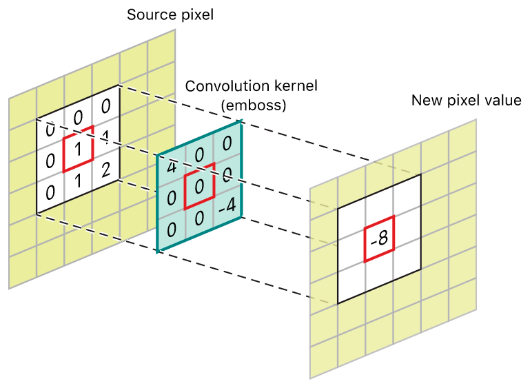
MACs require quite a few steps, for an n-by-n kernel one needs to perform n^2 multiplications and then n^2-1 additions to accumulate the values, so 2n^2-1 operations per MAC. On a conventional processor that can perform one operation at a time per clock cycle (yes, I know this isn’t how they really work), this means 17 cycles per pixel for a 3-by-3 kernel. This has to be repeated for every pixel in the image too! So that’s a lot of cycles, in reality there would be many more to move the data around the processor in addition to performing this math.
The reason it takes so many steps on a conventional processor is that they (generally) don’t have the hardware to perform a MAC in a single step, so it has to be achieved through these individual operations it has the hardware to perform. Using the configurable logic of an FPGA one can design the hardware that would be needed to perform a MAC in a single cycle! This was the crux of our project, getting the FPGA to do these operations in hardware. From there it would just be a matter of adjusting our kernel values to achieve different effects.
System Design
The first stage in any successful design is planning. For this project as is typically of digital systems projects this took the form of a block diagram where we outlined all the modules we would need and drew the flow of data through our system. From here we then divvied up tasks among ourselves. There were a few main sections that we identified:
- Camera interface - Responsible for getting the video data for us. Handled by one of us on their own.
- Image processing - Would apply a kernel to the video feed. Worked on by two members.
- VGA Interface - Would output the processed image for the user. I focused on this.
- Neural Network - Used to perform the digit recognition. Was combined effort from my three teammates.
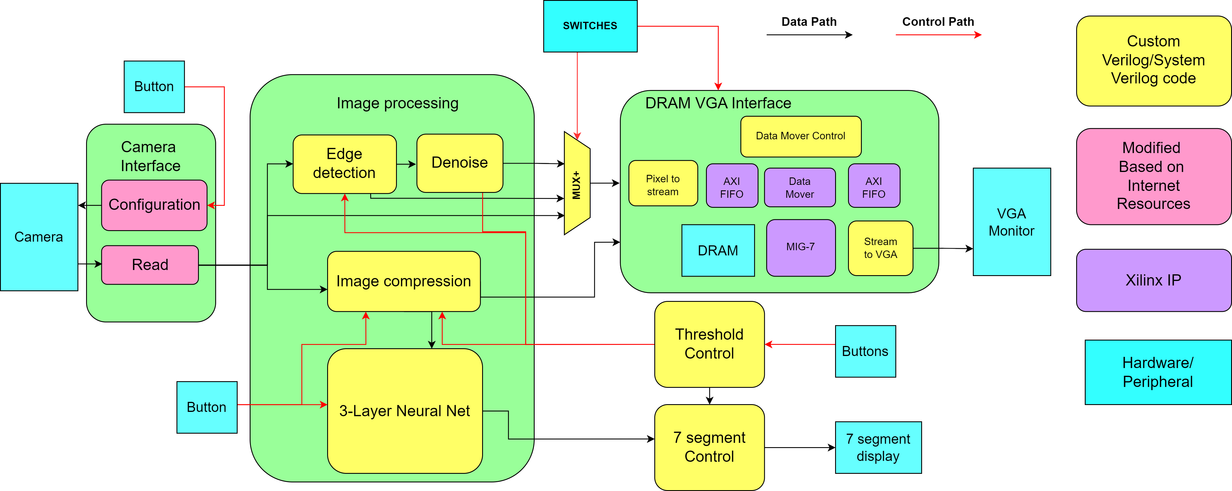
I focused on the VGA output stage to display the video. Another took the camera front end, and the other two focused on the processing. When we decided to add the digit recognition feature the three of them worked on the processing for that while I prepared the preview utility.
Camera Interface
This was relatively simple module that had two main parts: a configuration module to control the camera, and a module to read in the video from the camera. We actually sourced (and cited!) much of the camera code from an open source project1 we found online.
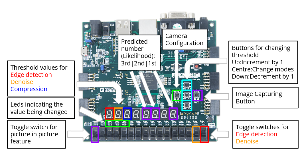
Camera Configuration
Configuration only had to be performed once to initialize the camera, from then on it would stream out the data as configured to. Communication to the camera took place over an manufacturer design SCCB protocol, which was a lightly modified I2C protocol. The configuration for the camera was hardcoded into a Read Only Memory (ROM) block on the FPGA as a series of target registers and values to write. This meant that to change the camera’s configuration we would need to compile a new bitstream for the FPGA, however we only had to change the configuration twice or thrice throughout the project so this was fine.
We assigned a button to trigger a camera reconfiguration in the event it was disconnected or some other issue required remedying.
Reading Video Data
Receiving the video data wasn’t too difficult. The data was already digitally transmitted to the FPGA so all we needed to really do was watch for the start of frame signal and then accept the pixels starting from top-left, going across to the right and then down, row-by-row, for the entire image.
Video Processing
This was the selling point of our project, processing a live video feed, ideally at full speed, with minimal latency. The processing we would be working towards was a kernel operation. Initially we planned to allow kernel values to be changed on the fly from a host computer, however we decided to simply load a couple of distinguishable presets on the FPGA and switch between them using the switches.
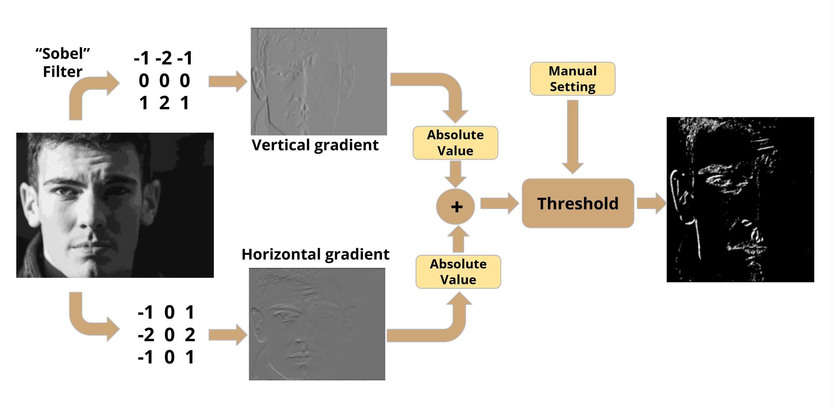
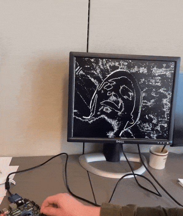
Our main example would be edge detection which we accomplished using a Sobel filter2. This approximates the gradient of an image’s intensity, which highlights sudden changes - edges. Then we would compare the magnitude of the gradient at each pixel to a threshold (user adjustable) to mark it as an edge or not.
Conversion to Greyscale
Although not shown in the block diagrams, one key component of the video processing pipeline was a conversion from a full colour (RGB) image to a greyscale one. The motivation for this was to simplify the processing that would follow since having multiple colour channels would make effects hard to administer in a visually coherent way and it didn’t even really matter for our intended result (edge detection and number recognition).
This was done by a simple pixel-wise operation on the pixel stream by combining their RGB values in certain portions.
Kernel Implementation
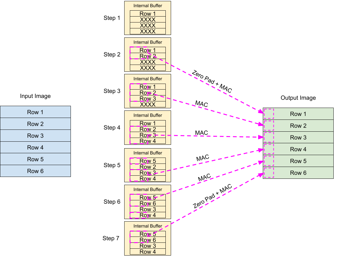
Writing the code to perform the MAC operation was trivial. The real meat of this portion was ensuring that the right data was being used. What I mean by this is that the camera sends the pixels sequentially from top left to bottom right, and each pixel only once. The MAC however needs to operate on a grid of pixels across sequential columns and rows, and pixels need to be used multiple times, so streaming pixels straight from the camera into the MAC operator wouldn’t work.
For this to work properly each kernel operator needed to buffer at least three adjacent rows which it would then scan through to perform the kernel operation on all the pixels. For our literal corner and edge cases where the kernel would extend beyond available pixel data, we would use zeros for the lacking pixels (“zero-padding”). In the end each kernel operator module had a buffer for four rows, so that one row would have data written to it while the other three were being computed on.
Testing the Kernel
The kernel worked as expected after a few iterations. However, due to the limited colour depth of the camera we had issues with getting noisy outputs for edge detection, especially in shaded scenes.
To clean this up, we made use of our kernel module once again, this time the kernel was set to count how many edge pixels neighboured other edge pixels. If a pixel didn’t have enough neighbouring edge pixels it was likely just noise/dithering along the transition of shades and ignored. We called this our DeNoise kernel/effect, fancy right?
Adjusting Thresholds
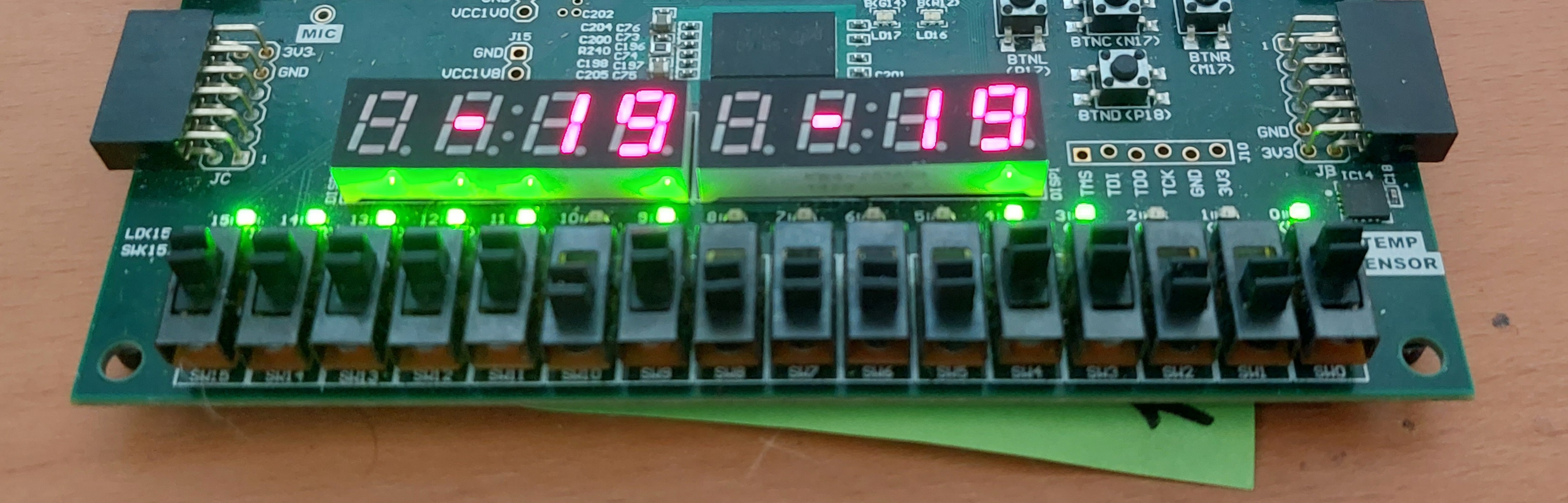
Since the comparison thresholds needed to be adjusted to suit the ambient lighting conditions so the system could operate optimally for edge detection and such, we made use of the buttons on the board to allow on the fly changes to be made and reviewed in real time. My contribution to this part of the project was writing the 80 lines of basic Verilog to output to the seven segment displays.
VGA Driver
Originally I (and the rest of my team) anticipated that the VGA portion would be a simple task since we would ideally just stream the video out at the rate it arrived from our VGA camera, and thus there would be no real need for a buffer. Once that was sorted I would join the guys working on the processing portion to help them complete that. Unfortunately, after some initial tests we quickly learned that was not going to be the case.
We anticipated that since our camera was marked as a “VGA” camera, with a resolution of 640 by 480 pixels, that it would output a video stream that could be readily displayed on a monitor that accepted VGA. The betrayal was that the camera had a VGA resolution - but not framerate. VGA monitors require a 60 fps input at that resolution, but the camera only output at 30 fps. So when we first tried to feed the camera data directly to a monitor it failed to be recognized as a video feed.
We would need a frame buffer to show each frame twice to bring the framerate up to 60. Not only that, but also we needed to do it right otherwise there would be visible artifacts if we were reading from the buffer as it was being partially written to (“screen tares”). This would need there to be two full frame buffers that we would alternate between reading and writing to, a “ping-pong” buffer arrangement. We did the math to see how much memory was needed to accommodate this: 12-bit colour depth, 640 by 480 (307 200) pixels, so 3 686 400 bits per frame. The FPGA had only a smidgen over 6 Mb so it would be unable to hold the frames, so it needed to go off-chip into the Dynamic RAM (DRAM).
To compound the complexity introduced in moving data off-cip, DRAM is mapped memory (each read/write needs an address), however the pixel data was provided as a stream and the VGA module expected a stream input so I would need to convert between these two methods of data transfer. Luckily there was an IP available to me from Xilinx which helped simplify the job for me, amply named DataMover. So I built out the expanded VGA system around it as the core.
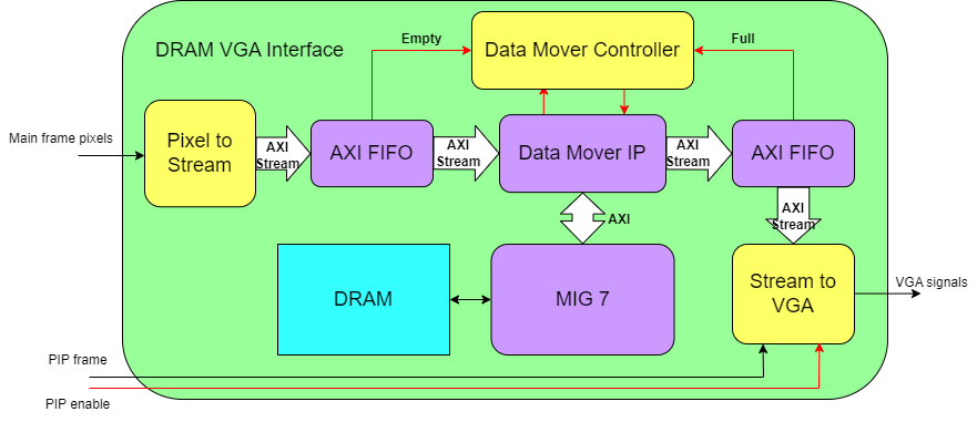
So, time for a tour of the trials and tribulations this system’s parts imparted on me.
Pixel to Stream
This part actually went quite easily, it was responsible for taking in the data for several pixels and combining them into one packet which was then sent forward over a AXI Stream interface towards the DataMover. The reason packets were collected like this was twofold: firstly packing them made more efficient use of space and bandwidth since each pixel needed 12-bits, not a nice multiple of 8 - secondly the image processing didn’t actually use AXI Stream interfaces, so there needed to be something that would signal the way DataMover expected inputs would be provided.
The only issue I had with this code was that I initially didn’t stage my inputs right. So if I received pixels too quickly and couldn’t offload them then some would be lost. This caused issues later because then the first few pixels from the next frame would fill in for these lost pixels, causing the last few rows in the image to look odd. Luckily when I went back to fix this once I determined the root cause I was greeted with this lovely past assumption.
// Look into adding a second internal buffer so the flow in isn't interrupted.
// Realistically the pixels are coming in at a rate about 12.5 Mpixels/second
// so this should be more than capable of handling it now

localparam PIXELS_TO_BUFFER = STREAM_WIDTH / 16;
Stream to VGA
This was the first part I started in the system since it was derived from my initial VGA driver code. Its function was pretty simple: take in a stream of pixels and put them up on the screen. Other than needing to unpack the pixels to undo what pixelToStream did, this was a pretty standard VGA output affair, I simply had it keep counters running off a VGA frequency (25.2 MHz) to know when pixels were meant to be broadcast, and others to know when to properly signal the end of a row or frame. Outputting colour data was done directly from the FPGA’s pins into a resistor network which feed the VGA interface.
It made use of a small AXI Stream buffer feeding it to smooth out the flow of pixels, accumulating them then VGA driver was in a blanking period and then doling them out quickly when pixels were being drawn.
I later expanded on this a bit to accommodate the preview of the input to the digit recognition system.
Memory Interface Generator (MIG)
This was a Xilinx IP and it connected directly to the DRAM interface/pins on the FPGA and the DataMover IP. We didn’t do anything else with it other than verify the range of memory addresses available since it was automatically configured to match what our development boards needed.
DataMover and Controller
This is where I spent a couple weeks tearing out my hair.
The purpose of these two modules was to move data from an AXI stream into a part of AXI mapped memory while reading part of mapped memory back into a stream. This was actually the express purpose of the DataMover IP, however the DataMover needed something to issue it commands on where to move data so that’s where my module came in. The commands the DataMover expected were pretty simple, they boiled down to essentially “Read/write X bytes to/from the AXI stream, starting at address Y in mapped memory”, simple enough eh?
I assigned two regions in the DRAM for the frame buffers and then started on laying out my logic for issuing these commands. There were two halves that operated almost entirely independently, Stream to Memory Mapped (S2MM) for putting video data into the frame buffer, and the Memory Mapped to Stream (MM2S) which then retrieved it for the VGA system. The only data exchanged across the halves was where the S2MM was writing to trigger frame buffer swaps. The logic for each half was similar and could be summarized as follows:
- Wait until the stream buffer in/out of the DataMover is ready for a transfer
- S2MM would wait until there was enough data was available for a complete transfer to DRAM (buffer not empty)
- MM2S would wait until the buffer had space for another transfer (buffer not full)
- If partway through a frame buffer, just issue an instruction to transfer the next block of data to/from DRAM
- If one half just completed a read/write of a frame buffer:
- S2MM would start writing the new pixels to the other frame buffer. This was safe to do, even if the other buffer was being read because the reads were done twice as fast as writes so the writes would never go ahead of the read point and cause artifacts.
- MM2S would check if the other frame buffer was completely written to or not. If completed, it would start reading that buffer, otherwise it would reread the buffer it was currently on.
- Once a command is issued to the DataMover by one half, that half waits until it receives a response confirming the completion of the transfer before issuing another
This base logic remained unchanged for the project, however due to quirks of the DataMover and also our system generally some minor additions were made.
Troubleshooting the Memory System
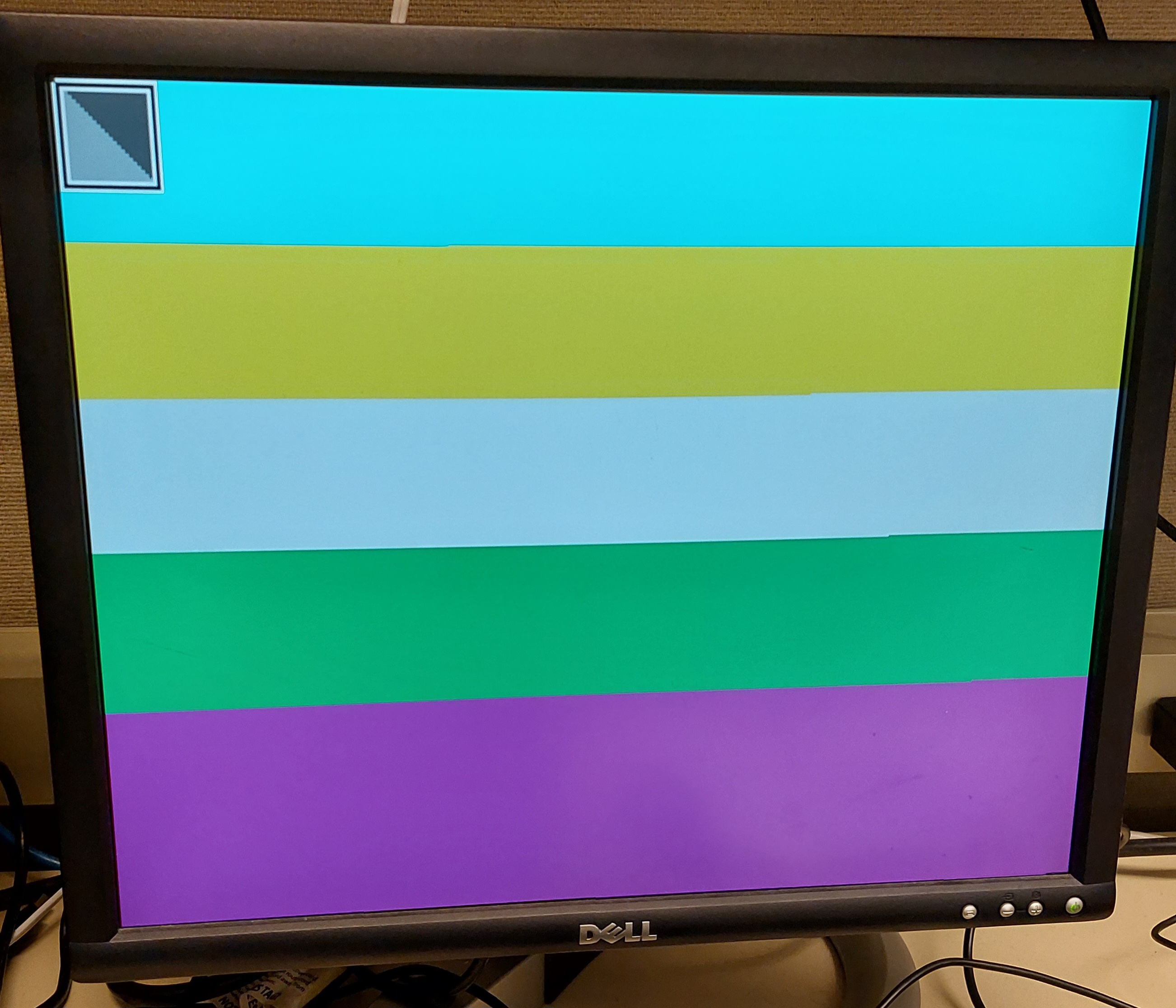
To develop the frame buffer system I worked without a camera. Partly because we only had one to share on our team but two FPGAs, but also because by using switches to simulate a pixel stream I had a better time noticing errors and glitches with a controlled input to the system. Since our system used 12-bit colour I used sets of four switches to set the value of each RGB colour channel. An additional switch was used to control if the frame buffer would accept the pixel values or not, which allowed me to “stop” the video feed and ensure that the frame buffering was working as intended by reading one frame repeatedly until the other was complete.
Since the pixels were streamed in from top left to bottom right the end effect of this system was that I ended up painting a lot of coloured bands in tests. I got nice sharp changes by pausing the pixel stream when changing colour settings. These tests helped me iron out issues I found with the DataMover IP, which I found two main ones.
AXI Data Bus Width
First issue was that when I increased the data bus width from 16 to 64 bits between the DataMover and MIG in an effort to reduce congestion the DataMover began skipping parts of memory when reading or writing, resulting in data “shingling”. When writing 64 bit messages that gradually increased in value on a 16 bit bus, the memory looked how one would expect: continuous data.
| Address | Bytes 0-3 | Bytes 4-7 | Bytes 8-B | Bytes C-F |
|---|---|---|---|---|
| 0x80000000 | 0x00000000 | 0x00000000 | 0x00000000 | 0x00000000 |
| 0x80000010 | 0x11111111 | 0x11111111 | 0x11111111 | 0x11111111 |
| 0x80000020 | 0x22222222 | 0x22222222 | 0x22222222 | 0x22222222 |
However once I switched to 64 bits it would write 32 bits, skip 32 bits, then write the remaining 32 bits. This was evident thanks to the clearly uninitialized data blocks when reviewing the memory map.
| Address | Bytes 0-3 | Bytes 4-7 | Bytes 8-B | Bytes C-F |
|---|---|---|---|---|
| 0x80000000 | 0x00000000 | 0x00000000 | 0xDEADBEEF | 0x13371337 |
| 0x80000010 | 0x11111111 | 0x11111111 | 0xCAB0CAB0 | 0x8BADF00D |
| 0x80000020 | 0x22222222 | 0x22222222 | 0x0420FACE | 0xDEADFA11 |
I remedied this by simply adding a factor used in address calculations to double the step for each transfer to account for this skipping since at least the DataMover did this skipping on both the write and reads. So the memory would now look like this.
| Address | Bytes 0-3 | Bytes 4-7 | Bytes 8-B | Bytes C-F |
|---|---|---|---|---|
| 0x80000000 | 0x00000000 | 0x00000000 | 0xDEADBEEF | 0x13371337 |
| 0x80000010 | 0x00000000 | 0x00000000 | 0x0420FACE | 0xCAB0CAB0 |
| 0x80000020 | 0x11111111 | 0x11111111 | 0x8BADF00D | 0x69696969 |
| 0x80000030 | 0x11111111 | 0x11111111 | 0x0D15EA5E | 0x01234567 |
| 0x80000040 | 0x22222222 | 0x22222222 | 0xDEADFA11 | 0xD0D0CACA |
| 0x80000050 | 0x22222222 | 0x22222222 | 0xBADDCAFE | 0xB0000000 |
Troubleshooting VGA with the Camera
With the VGA memory system seemingly ready, we began tests using the camera feed. Immediately we found an annoying issue where the last few columns for the rightmost part of the frame wrapped around and became the leftmost ones displayed. Unfortunately I didn’t bother to take a picture at the time. After some experiments we were able to trace the root cause, for some reason the last 32 bits of what was meant to belong to one frame’s buffer was the first 32 bits of the other and vice versa, so reading them resulted in this shifted image.

Initially we tried to offset the transfers by one when reading from the frame buffer to try and counter this but then it just started wrapping the other way.
DataMover Internal Buffer
After some more thorough analysis I was able to pin the culprit - once again it was my good friend DataMover.
To test it I wrote a basic module that would alternate between feeding the DataMover frames that were all white or all black so I could easily know how the data for each frame was intruding on the other. After probing the memory map as I had for the previous issue, I found the cause was something related to the stream being shifted relative to what was anticipated, which aligned with what we could see. However there was one thing that was odd about it, the intrusion wasn’t a whole transfer’s worth of data (8 packets, 64 bits wide, 64 bytes) but half that at 32 bytes. This explained why shifting the transfer by one resulting in the wrap reversing the direction. However this number didn’t make any sense to us for two reasons:
- Our transfer commands for both S2MM and MM2S were hardcoded to be 64 bytes every time, why was it off by 32 bytes?
- Why did carry perfectly between the two frame buffers? The weren’t adjacent in memory.
After a bit more probing I probed the AXI bus to spy on what was happening. The data coming out of the DataMover had this shift to it, so the MIG was not at fault - it had to be happening inside the DataMover itself. After some thinking I realized there must be some internal buffer on the S2MM side for 32 bytes, even though I explicitly set up the DataMover to not have internal buffering. These 32 bytes led the first transaction after reset and thus caused all following data exchanges to be shifted accordingly hence the wrapping.
I couldn’t find out how to remove this internal buffer in the IP, so I tried to counter it on the S2MM side by repeating the first 32 bytes worth of data of the first frame following a reset to try and bring the memory to a state as though there was never this initial shift. However then I also needed to have logic to do something similar at the end of a frame to flush out the last few pixels before the next frame started to arrive. The logic for this quickly grew complicated and filled with bugs so I canned it and decided to try and handle it on the MM2S side.
Handling it on the MM2S side was easier and ultimately the way I kept it, even if the memory map didn’t exactly work perfectly. What I did was I simply had the system read a frame as it normally would from the start of a frame buffer to the end, discarding the first 32 bytes to avoid wrapping from the other frame’s data. To get the last 32 bytes for the image it just read the first part of the other frame buffer where they would be due to this shift. This was safe to do since the MM2S would only switch once the S2MM would start writing to the other buffer, and these bytes were always in the first transaction that would mark this.
With that ironed out the VGA driver was at last complete
Digit Recognition
We had all the parts complete for our original design to a reasonable level with a couple weeks to spare in the project so we decided to attempt introducing a character recognition system. This wasn’t as outlandish of a feature for us to implement as would first sound. Firstly, it was obviously still tied to our image processing goal, but a second more subtle reason is that some neural network schemes themselves, especially for image processing, operate using kernels/MACs!
I personally wasn’t super involved in the development of this portion as I was still wrangling the last few bugs in the VGA system at the time. My contributions to this outside helping brainstorm solutions for some of the issues was in adding the previewer for digit images over the live video feed, so for the other parts I am drawing on what I was told and was written in our final report.
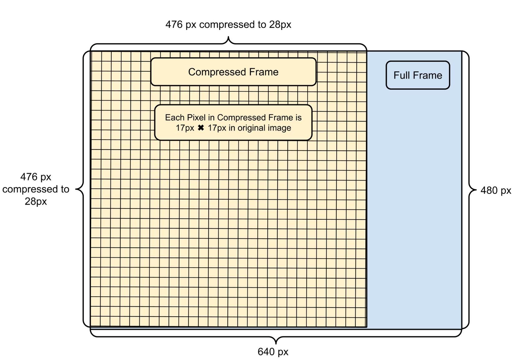
Image Compression
Compressing a video frame from full VGA resolution, 640 by 480 pixels, down to 28 by 28 pixel image prior to conducting the digit recognition allowed us to use a much smaller neural model without sacrificing accuracy. The reason we chose 28 by 28 specifically was that our model would be trained using the MNIST database for written digits which used this resolution (more on that in the neural network section).
Our compression algorithm followed a couple of steps to properly convert the image into something to be processed:
- Sum all the pixel intensities in 17 by 17 pixel blocks to create a 28 by 28 grid. Pixels outside this region in the original image are discarded.
- Find the maximum and minimum sums in this region. E.g. 100 and 1600.
- Scale the values of the sums so that those at the minimum are 0, those at the maximum are at 15. \(x = \frac{x - x_{min}}{x_{max} - x_{min}} * 15\), so using the example values 200 would become 1. This allows us to maintain the dynamic range of the image.
- Invert the scale, since the training data used white on black digits while we were using black on white. \(x = 15 - x\)
- Compare values to a threshold, if below the threshold floor the value to 0. This was to combat the background being non-uniform due “vignetting” where the edges of an image are darker compared to the center.
Neural Network
This is where my understanding of my teammate’s work gets really murky, so really digging through their parts of the report for this.
To accomplish digit recognition, we prepared a three-layer neural network. The first layer was a 1 by 784 matrix so there would be a factor for each pixel in the compressed image, this then connected to the first hidden layer of 784 by 10 factors, which then went through two additional 10 by 10 layers to provide a probability of a given digit 0 to 9 being present in the image. The digit with the highest probability of being present was then suggested as the digit present but we also displayed the second and third most likely candidates.
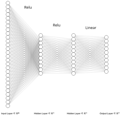
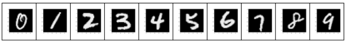
As labelled in the diagram, the hidden layers used ReLU activation, but the output layer was computed using a linear operation. To train the network we used the MNIST database3, which contains a collection of handwritten digits represented as 28 by 28 pixel images.
Training for FPGA Deployment
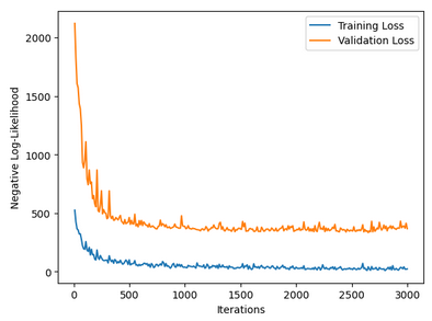
My teammates used gradient descent to train the network parameters, which they ran for 3000 epochs at which point the losses were clearly decreasing. The model at this point achieved about 90% accuracy on the training data.
At this point we had to begin adjusting how the neural network would operate to work better on the FPGA. Firstly we decided to use 10 by 10 matrices for the intermediate layers instead of 20 by 20 since that would have quadrupled the memory requirements but only improved accuracy by about 3%.
With the trained model prepared and selected, we began by converting the weights from floating point numbers (e.g. 12.674) to 16-bit integers for easier multiplication and accumulation in the FPGA. 16 bits were chosen since this balanced accuracy with speed on the FPGA since we wanted to make use of the Digital Signal Processing (DSP) blocks which accelerate multiplication and they can only take in integers up to 16 bits wide. Converting the floating point values to integers has one main issue, it discards information after the decimal point which can result in a loss of accuracy. To minimize this loss my team aimed to space out the factors so that casting them to integers would not result in a loss of accuracy, while staying within the bounds of 16 bit signed integers (-32 768 to +32 767 inclusive). To accomplish this my team made use of two tricks:
- Scaling the training database. Making the training data more coarsely spaced by scaling everything by a factor will generally result in more coarsely spaced parameters.
- Scaling the final parameters. Since our entire network is linear, except for the ReLU activation function (which is close to being linear), scaling all the parameters by a constant factor does not affect the classification output. This can help bounding the weights to fit in a 16-bit signed integer without needing to retrain.
Executing the Neural Network on the FPGA
This part wasn’t really as exciting or novel compared to the preparation for it. For each layer we implemented finite state machines with three main states executed in this order:
- Multiplication by the model weights
- Adding biases from the model
- ReLU (if needed for that layer)
The multiplication for the first layer was done per pixel sequentially, requiring 784 cycles to complete since there weren’t enough DSP blocks on the FPGA (430). However the later layers only needed to multiple by 10 factors each so these were entirely parallelized so they completed in a single cycle each when the data from the prior layer was complete.
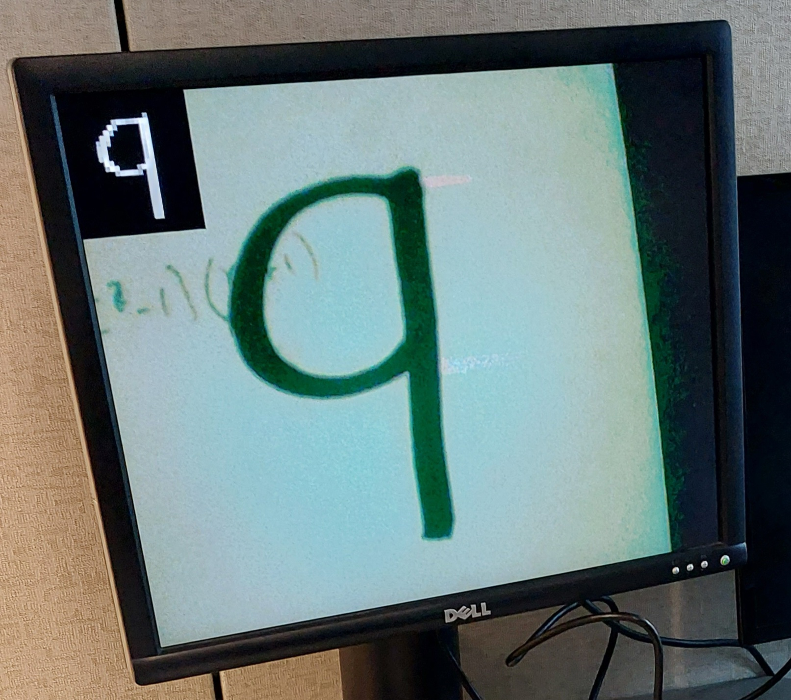
Digit Preview
To aid with the testing and operation of the digit recognition system I contributed a system to preview what the digit processing model was being provided. This was a up-scaled version of the compressed image overlaid over the live video feed in the top left corner if enabled, so we could see how well the digit looked and if any thresholds needed adjustment. The reason for upscaling was to make it more legible since 28 pixels is quite small even at VGA resolution. Given the way it looked, I referred to it as “picture in picture” or PIP for short.
To get this to work I modified my VGA driver block. If the signal was received that the preview was needed on screen then it would simply discard the video stream pixels in the top left and replace them with the appropriate pixels from the compressed image buffer on the FPGA. I managed this by using counters to keep track of where I was in the output image and some comparisons to multiplex between the pixel stream of the video and the buffered image.
Outcome
We not only managed to complete our original vision of live video processing successful in hardware, but also managed to tack on the digit recognition feature which worked decently! It was really satisfying to see our system work live and then demonstrate it to the course instructors and classmates at the end. We recorded a short demo of the system and submitted our final report which was well received, you can read it here.
Tips for Others
As part of our report, we were asked to identify some tips that we would like to share with other from our experience working on the project. I would suggest you them there if you want all the details but in summary we had advice on three main topics:
- Using the DataMover IP
- Given its well-known peculiarities in behaviour, one should spend more time considering whether or not to use it compared to other alternatives like the open source WB2AXIP project
- If using the DatMover IP, verify that your transactions are being done as expected by probing the memory.
- I caught it skipping regions of memory, resulting in me “shingling” the last parts of early packets with the start of later packets
- I used a MicroBlaze processor with a “Hello World” program and debugger to view the memory map to do this
- Check if the DataMover is buffering data internally and how much
- I noticed it was storing half a burst’s worth of stream data internally with no clear way around it so I had to work around this to properly read the image buffer
- Running neural networks on an FPGA as mentioned in its section
- Convert weights to integers
- Try to scale weights to make the most of the available acceleration hardware on the FPGA like DSP blocks
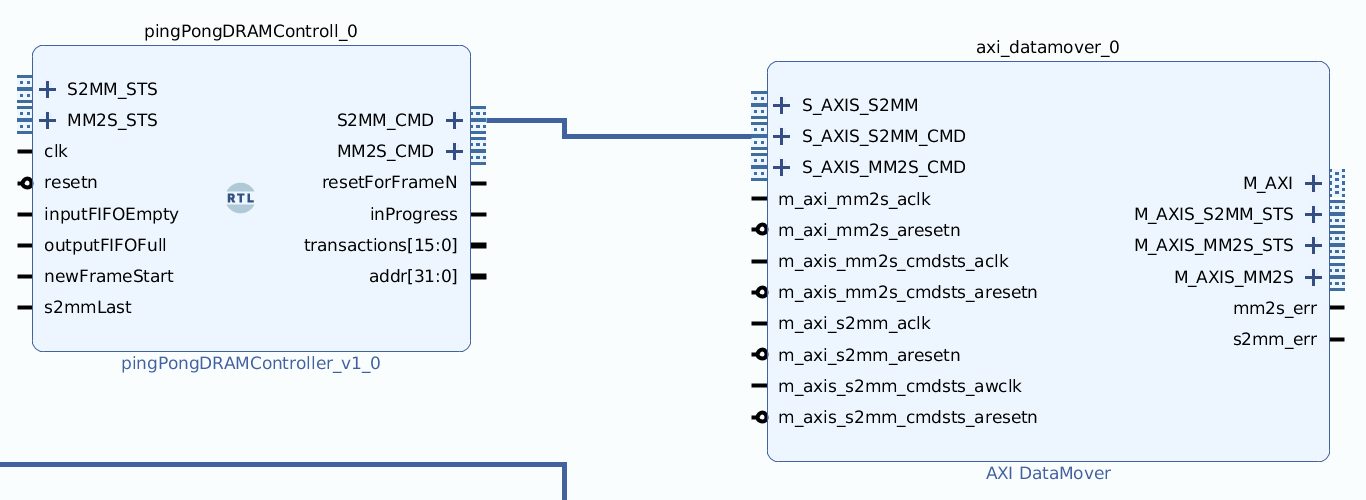
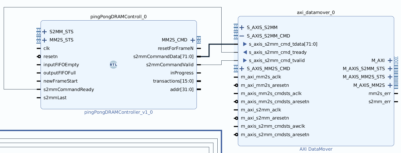
- Use standard interfaces between modules, especially for block diagrams!
- Helps ensure data is moved around correctly
- Can tidy up large block diagrams by bundling all signals for an interface
- Below is a code snippet for how to do so for a AXI stream interface
// S2MM Command Port - AXI-Stream interface named "S2MM_CMD"
(*X_INTERFACE_INFO= "xilinx.com:interface:axis:1.0 S2MM_CMD TDATA"*)
output [71:0] s2mmCommandData,
(*X_INTERFACE_INFO= "xilinx.com:interface:axis:1.0 S2MM_CMD TREADY"*)
input s2mmCommandReady,
(*X_INTERFACE_INFO= "xilinx.com:interface:axis:1.0 S2MM_CMD TVALID"*)
output s2mmCommandValid,
-
OV7670-Verilog by Weston Braun. Available: https://github.com/westonb/OV7670-Verilog ↩︎
-
Sobel Operator on WikiPedia - https://en.wikipedia.org/wiki/Sobel_operator ↩︎
-
MNIST Database on Wikipedia - https://en.wikipedia.org/wiki/MNIST_database. The original source by Y. LeCun and C. Cortes (http://yann.lecun.com/exdb/mnist/) needs credentials to access. ↩︎