ESC V4
Table of Contents
Overview
While V3 was meant to be a partial solution to some of the issues I had with V2, V4 is meant to fix everything with some radical changes. New microcontroller family, changes to the output stage and BEMF, etc. The main change is the new family of microcontroller used, tinyAVR 1-series, with the ATtiny1617 specifically.
This change in microcontroller was fuelled by both the advantages it brought (features, cost) as well as the scarcity of new ATmega328P or PB chips at the time prohibiting me from getting new ones for more V2 or V3 boards. Other hardware changes arose from me gaining an understanding of each part of the system and how to improve them.
Development was going well, much of the code could be reused with changes only to reflect the different registers used on the ATtiny1617 compared to the ATmega328P(B). Unfortunately I was unable to do too much testing and development as I accidentally fried the last remaining MOSFET drivers I had available to me before I got to actually spinning the motor.
Takeaways
- I need to pay more attention to transients when commutating the motor
- Using dedicated programming hardware is a massive leap in quality of life
- I could add a status LED in a future version
Detailed Report
This was meant to address all the issues I had with V2, primarily by changing the brains of the system as well as a few touch ups to various parts. Resiging the circuit and porting/updating the code was a pretty involved process and I would equate the work put into this to what I did making V2 even if it is based off it.
Although I started work on it and had some preliminary designs done in September 2020, I didn’t work on it much from then until June/July 2021 due to my studies filling my time.
Circuit Design
The circuit has functionally has four main sections: microcontroller, headers, output stage, and a network for feedback from the motor. I’ve sectioned off the schematic with explanations for each, but to summarize:
- The microcontroller section is responsible for controlling the operation of the ESC
- The output stage recieves signals from the microcontroller and drives the motor accordingly
- The feedback network (labelled as “BEMF Dividers” in the schematic) is responsible for preparing the signals from the motor for the microcontroller
- Headers are needed for connecting the ESC to either the rest of a system or for programming/debugging.

Microcontroller
The first order of business in this version was to select a new microcontroller to use in this design. The reason for this was that I was reaching some limitations in the hardware regarding timers, but more pressing was that I was unable to find any ATmega328P or PBs in the near future (I even wrote about the seemingly global shortage of these chips, little did I know how hard it would quickly become to get any chips in the future). To start my selection process I outlined my needs and wants for the new chip.
Needed:
- 8 kilobytes of flash
- 512 bytes of memory
- 6 Digital out
- 3 hardware PWM output
- 4 Digital in
- I2C interface
- Serial interface (can overlap with I2C)
- Internal analog comparator
- 1 reference pin for “zero”
- 3 other inputs for phases
Optional:
- Separated and simultaneous, I2C and Serial support
- 1 digital input with interrupts (for PWM in)
- 6 PWM digital out instead of just 3 of 6.
This required a chip with at least 18 pins (including power pins), or 21 for all I additionally want to be met as well. I decided to try and stick to AVR microcontrollers since those are what I was most familiar with, and I figured would be easier to port my code to since I made use of hardware registers. I was open to others though, as long as I could easily use them within some free development suite.
In the end I found the ATtiny 1-series, which not only had chips that exceeded requirements, but also were cheaper than the ATmega328P I was previously using! Specifically, I selected the ATtiny1617. It had some other features that make it nice to use, such as a smaller package overall and an internal calibrated 20MHz oscillator.
One thing I had to prepare my board for was a new programming interface since the ATtiny only supports UPDI programming unlike my previous projects which largely were SPI based. This meant I nbeeded to change that headers as well as prepare a new method to program boards.
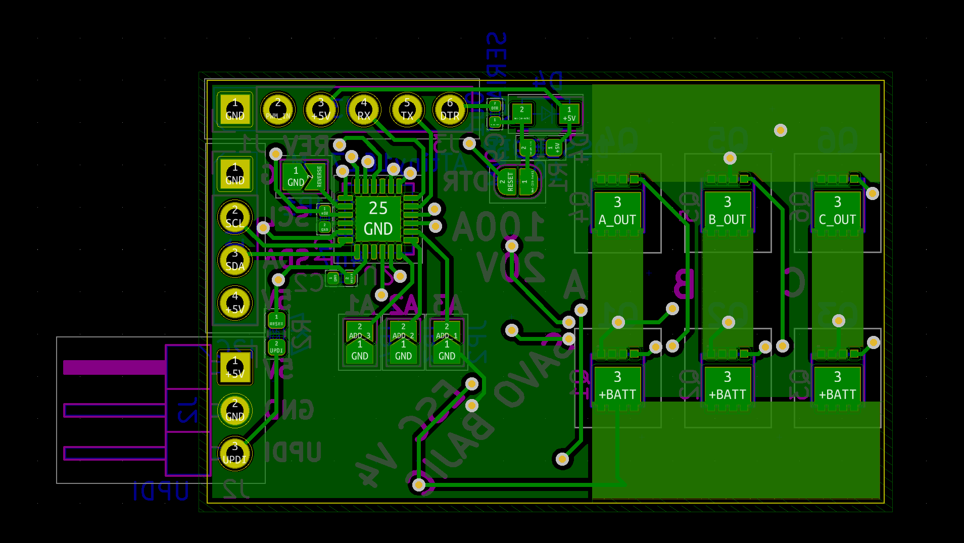
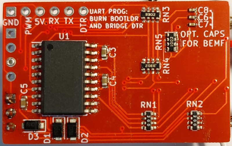
Microcontroller Section Design
Around the microcontroller there are some supporting components, namely decoupling capacitors and solder pads for settings.
When it came to assigning pins it was very helpful to use the very configurable nature of the ATtiny’s peripherals which allows most to be multiplexed to alternative locations. A notable example of this is when in my initial design stages I was using PC5 for PWM2 to the MOSFET driver. However, I was cheking vendors for ATtiny1617s and found that the automotive grade version has PC5 entirely disabled for any GPIO, so I used multiplexing to be able to use PWM2 coming out of PB5 instead. By doing this I can use the same code regardless of the version of ATtiny1617 I get.
Headers
The connectors and headers are used to interact with the board, of the three headers, two are for mainly just for development purposes, the third for control in the drone.
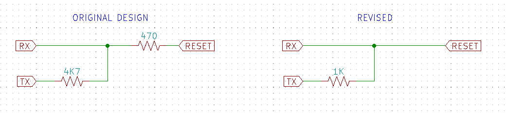
The programming headers have additional passives to enable programming. The UPDI header has a 470Ω resistor used to allow the chip to be programmed using a USB-to-Serial adapter with some some tricks with pyUPDI. (This 470 Ω resistor was revealed in revised documentation to be the wrong value). The Serial (UART) header is used for more conventional Arduino-like programming once a bootloader is flashed to the chip.
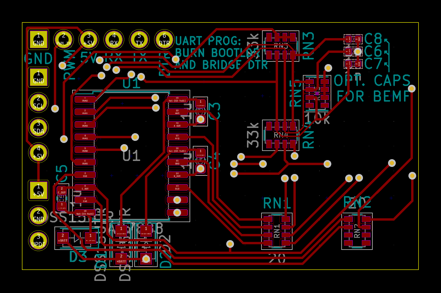
Output Stage
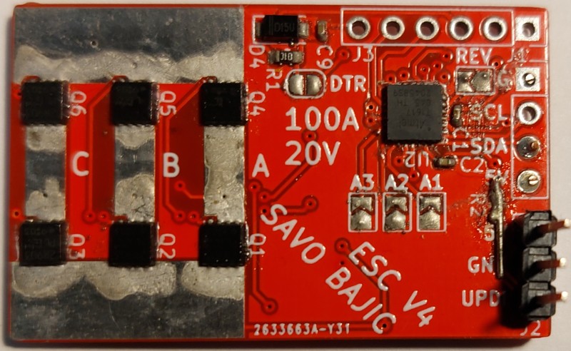
The output stage to drive the motor is fundamentally the same as the one present in all previous versions. It is a three phase inverter made of TPN2R903PL N-channel MOSFETs, driven by a single FAN7888 MOSFET driver IC that receives control signals from the microcontroller. The FAN chip is able to drive the N-channel MOSFETs through a process called bootstrapping which is essentially using using capacitors and diodes to drive the gates of these MOSFETs above the supply voltage.
There are some minor differences in this iteration though, related to the value of the passive present.
- Gate resistors, RN1 and RN2 in all versions, were reduced from 100 Ω to 20 Ω. This will allow them to charge the gates as fast as they safely can.
- Bootstrapping resistors, RN3 in previous versions, were removed entirely as they were not truly needed.
- Bootstrapping capacitors, C2-4 in previous versions, C3-5 in V4, were reduced from 4.7 uF to 1 uF as 4.7 uF was excessive.
The calculations and resaoning for these changes I found in onsemi’s application notes AN-6076 and AN-9052 which cover the design and component selection of bootstrap circuits respectively.
Feedback Networks
The networks of passives used for conditioning feedback is built up from previous versions. The same resistors are used to divide the phase voltages down to a safe range for the microcontroller and providing the average. I added smoothing capacitors to remove the noise from the signals for this version. These are capacitors C6 to C8.
Layout
I kept the overall size of the board identical to the previous two versions since I felt it was the right size. Although I rearranged some of the parts per side of the board, the overall component grouping stayed the same from previous versions as well.
Looking at the layouts now as I write this I realize that although the functions grouped by side have remained the same from V3 and V2 (driver and resistor networks, microcontroller and MOSFETs), I for some reason seem to have flipped which group was on which face. Doesn’t matter really though as “top” and “bottom” are relative terms anyways and will not affect the function at all.
Everything used for the ESC is surface mount to help keep the overall size of the board smaller, not only because of their generally smaller nature, but because they solder to pad on the surface it allows parts to populate both sides of the board without interfering with the opposite side. The only exception are the headers along the edges since it is a much better joint mechanically when soldering in a hole compared to a pad.
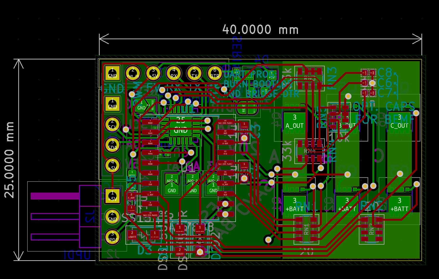
The top side of the board houses the MOSFET driver circuitry on the left half and the feedback network on the right. I added some text to the silkscreen to help clarify some of the connections and provide guidance to me.
Given the reduced number of components in V4 compared to V3 or earlier, the bottom side, where the control electronics and MOSFETS reside, is quite simple. Given this additional space more notes are available on the silkscreen.
Assembly
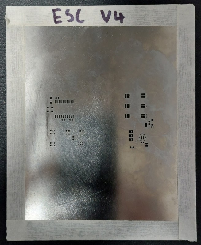
The assembly for these boards was pretty routine. I ordered the board, components, and a solder paste stencil specifically for this board and got to work; pasting, placing, and reflowing.
The only thing that didn’t work out nicely for me during the assembly phase was that when I was ordering everything in the summer of 2021 I was unable to get new MOSFET drivers due to shortages, so I had to use the leftovers from my V2 assembly days and even harvest the functional ones from previously assembled ESCs. (Is this foreshadowing a future issue?)
The final assembled ESC V4s came out looking pretty good. Here is the “top” with the MOSFET driver and feedback array.
A view of the control/MOSFET side of one assembled ESC V4. Note: R2 was originally installed, but was replaced with a short when I started using a ATMEL-ICE programmer.
Testing
Testing followed the same scheme as it did when testing V2. With my experience working on V2 and my improved understanding of the systems I was working with, the basic power tests were completed quickly and without issue. Using a new and hacky programming method for the UPDI was were I started to hit issues.
Working with UPDI
I had never encountered UDPI before this project. So when I was looking up open-source/free tools for uploading to a UDPI target I came across pyUPDI which was exactly what I needed. Something simple and easy to implement in both hardware and software.
UDPI stands for Unified Program and Debug Interface, an it uses a single pin on the target microcontroller to achieve all this. pyUDPI uses a standard USB to Serial adapter and a couple of resistors to interface with the target chip, and then some python scripting on the host PC to simulate the communication protocol.
Initially I followed an outdated guide that instructed me to use a 470 Ω resistor between the UDPI pin on the target and the programmer as well as a 4.7 kΩ resistor on the TX line from the Serial adapter. This did not work. After some more testing and eventually finding a more up to date guide, I revised my design to the new recommended version with just a single 1 kΩ resistor between TX and the other pins.
This worked, although at a very slow upload speed of a couple hundred bytes a second. But hey, it worked!
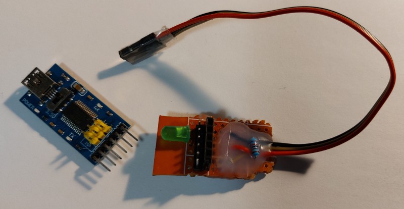
I took the circuit from a breadboard and decided to give it a proper permanent home on some perfboard. I soldered all the required components on, with headers to accommodate either style of connection to USB-to-Serial adapters. I also added a green LED that would only light up when the adapter was correctly inserted, to prevent careless mistakes.
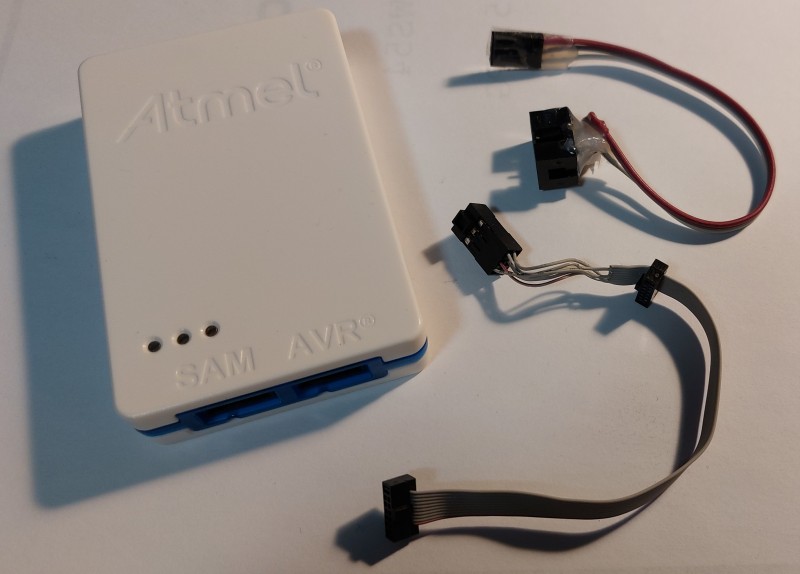
Our time together was not meant to last, and I grew frustrated with the upload times that exceeded 30 seconds for code that was merely a few kilobytes. In the end I decided to splurge and bought myself a proper programmer for ATMEL chips. It makes sense as my ambitions grow and I want to try and make the most of my projects. I had to prepare a little adapter to bridge my 3-pin UDPI header to its 6-pin connector.
The upgrade in tooling spoke for itself immediately! My programming times were a fraction of what they were using my pyUDPI arrangement (<2 seconds compared to >30 with pyUPDI), and since it was isolated from the board’s power I didn’t need to worry about leaving it plugged into the board when I shut down power. For future revisions I may reinstate a small (linear) 5 V regulator to power the ESC control again. With a provision to easily switch to an central 5 V supply as desired.
Motor Testing
With programmed settled, and running through the same basic tests for features like PWM or analog comparators run the same as they were for V2 (e.g. potentiometers for analog comparators) - I had to set up testing with the motor. This once again started by me repeating myself from working V2. I reused the motor and resistors from the V2 tests and went about trying things out.
During these tests as I was tuning the buzzing feature, I fried the last of my MOSFET drivers. This was before I could properly test normal motor operation! I was able to find an alternative driver in the same packaging, but it they did not share the same pinout, so I needed to make a new revision in order to have the traces properly routed. Cue V5!
Developing Firmware
Once I was able to upload code to the ESC I began my efforts to port the firmware from V2 to V4. I followed an order modified to how I originally developed the firmware for ESC V2:
- Implement hardware PWM
- I2C communication/control
- BEMF detection (zero-point crossing handling)
- Commutation
- Buzzing on the motor
- Running the motor (never reached)
In addition to porting to accommodate the new hardware, I also switched to using the PlatformIO IDE in VS Code from my old friend, the Arduino IDE. The reason for the IDE change was to provide me more of the creature comforts modern IDEs offer such as easier code navigation and auto-complete to name a few. The code would still be built in the Arduino framework so I would still have access to the functions and libraries offered by default in the Arduino IDE, such as “millis()”.
Implementing Hardware PWM Control
I designed the ESC such that all the MOSFET control pins were controlled by a single timer, the zeroth timer/counter type A, or as one can more affectionately call it - TCA0. This is a 16-bit timer that has three compare thresholds, however to control all six of my PWM outputs I operate it in “split” mode which divides the 16-bit counter and thresholds in two, which are referred to as “lower” or “higher” halves and provide the six outputs I needed.
I control the timer by directly writing to the resisters. Below is the code snippet I use to configure the timers.
TCA0.SPLIT.CTRLA = TCA_SPLIT_CLKSEL_DIV16_gc | TCA_SPLIT_ENABLE_bm; // Enable the split timer with prescaler of 16
TCA0.SPLIT.LPER = maxDuty; // Set upper duty limit
TCA0.SPLIT.HPER = maxDuty;
TCA0.SPLIT.CTRLESET = TCA_SPLIT_CMD_RESTART_gc | 0x03; // Reset both timers
To then actually set a pin to output the PWM wave we can use something like the following line. This line specifically forces the pin corresponding to the zeroth threshold on the lower half of the counter (PWM0) to follow the wave generated by that.
TCA0.SPLIT.CTRLB = TCA_SPLIT_LCMP0EN_bm; // Turn on PWM0 output (B high)
My tests with the hardware PWM were successful. I was able to have PWM running all on pins with different duties for each. I was also able to adjust the period on each half of the timer too. I prepared some functions to easily adjust all the periods in unison and also the setup function for the motor driver to include what was needed.
I2C Communication
This was pretty trivial to port compared to the rest of the system. Since it was entirely written using the abstractions afforded by the “Wire.h” library I didn’t have to change a line of code from V2 and it worked!
I did have to add a line of code to the setup function for I2C instructing the ATtiny1617 to use the alternative pins for I2C instead of the defaults. I was using the defaults for controlling the MOSFET driver.
Zero-crossing
Just like with the ATmega328P/B used in previous versions, I will employ an internal analog comparator in the ATtiny to monitor for zero-crossing events. Of the three available on the chip, I ended up using Analog Comparator 1 (AC1) since the pin allocations were favourable.
Just like with PWM, I wrote code that would interact directly with the registers related to the analog comparator. To set it up I would use the following code.
AC1.INTCTRL = 0; // Disable analog comparator interrupt
AC1.MUXCTRLA = AC_MUXNEG_PIN0_gc; // Set negative reference to be Zero pin (PA5)
AC1.CTRLA = AC_ENABLE_bm | AC_HYSMODE_25mV_gc; // Enable the AC with a 25mV hysteresis
To select the inputs to be compared I need to multiplex them to have them properly connected to the comparator. This is done using the MUXCTRLA register. The negative reference for the comparator is always the zero pin (negative pin 0), the phase of interest is connected to the positive input. This line sets the negative multiplexer to PIN0 (zero) and the positive to PIN1 (phase A).
AC1.MUXCTRLA = AC_MUXPOS_PIN1_gc | AC_MUXNEG_PIN0_gc;
This code proved to work properly during tests where I used a potentiometer to sweep across voltage ranges like I did previously and printed the output of the voltage regulator over serial.
However my work with the analog comparator was not complete. I still had some plans for how to improve the commutation system I used previously by tying it directly to a timer.
Commutation
My commutation code makes use of a function to set the phases for each of the six steps. Setting the right phases high and low and leaving the last phase floating. Doing it this way will also allow me easily add additional steps to this such as synchronous switching when the high phase is left floating during the “low” of the PWM cycle. Currently my function for each step looks like this, using my code to set A high, B low, C floating as an example:
void AHBL() {
  // Set up PWM pin(s) for high side
  TCA0.SPLIT.CTRLB = TCA_SPLIT_LCMP2EN_bm;

  // Set pin for low side and leave others cleared
  PORTB.OUTCLR = PIN0_bm | PIN1_bm;
  PORTC.OUT = PIN3_bm;
}
In addition to setting the phase outputs, I also needed to properly configure the comparator for each step to trigger at the zero crossings for each step. This just needed me to change which inputs were multiplexed. An example function at this stage was just:
void aRisingBEMF() {
  AC1.MUXCTRLA = AC_MUXPOS_PIN1_gc | AC_MUXNEG_PIN0_gc;
}
These function are pretty basic so when I tested them for the first time they worked exactly as expected.
Reversing
The reason I had the BEMF and commutation functions separate instead of combining them in one function for each of the six steps is so I could easily reverse the direction the motor turns in software. This is because although the order of commutation steps gets reversed, the zero-crossings edges to spot get inverted. A “forward” commutation sequence:
| Step | High Phase | Low Phase | Zero Crossing Edge Type |
|---|---|---|---|
| 1 | A | B | C↓ |
| 2 | A | C | B↑ |
| 3 | B | C | A↓ |
| 4 | B | A | C↑ |
| 5 | C | A | B↓ |
| 6 | C | B | A↑ |
Compare that to a “reversed” rotation:
| Step | High Phase | Low Phase | Zero Crossing Edge Type |
|---|---|---|---|
| 1 | A | B | C↑ |
| 2 | C | B | A↓ |
| 3 | C | A | B↑ |
| 4 | B | A | C↓ |
| 5 | B | C | A↑ |
| 6 | A | C | B↓ |
To keep my interrupts for commutation simple, and thus quicker to execute (and making my system more responsive) I simply have them call the functions stored in an array of function pointers, with each entry corresponding to the function needed at that particular step. This way I can easily programmatically rearrange the functions and thus rotation on the fly like any other variable array.
sequenceStep++;
sequenceStep %= 6; // Loop around at 6

motorSteps[sequenceStep]();
bemfSteps[sequenceStep]();
Commutation Timing
A critical component of the system is having the right delay after a zero-crossing to the when you commute the motor to the next step. This delay needs to be equal to the time it took to reach the zero-crossing from the previous commutation. In V2 this was done with two separate timer and analog comparator interrupts. However given the new features on the ATtiny1617, I can do it all with just one interrupt on the timer I use.
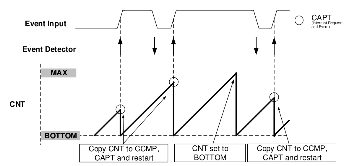
For timing I will be using the zeroth Timer/Counter Type B, TCB0. This timer has more features than what I had available on the ATmega328P. Among these is a new mode called “Input Capture Frequency Measurement”, which as the name implies is used to catch the frequency (well really period) of an event. When an event is detected, the current count is stored in the compare register before flagging an interrupt and restarting the count. Here is figure 21-6 from the ATtiny1617 data sheet to help explain it.
The neat thing about the ATtiny is that it has an internal Event System that is capable of routing a variety of sources to destinations. Using this I am able to route Analog Comparator 1 to be the event source for TCB0 with just few lines:
TCB0.EVCTRL = TCB_CAPTEI_bm | TCB_EDGE_bm; // Enable event capture input (AC), on falling edge
EVSYS.ASYNCCH0 = EVSYS_ASYNCCH0_AC1_OUT_gc; // Use comparator as async channel 0 source
EVSYS.ASYNCUSER0 = EVSYS_ASYNCUSER0_ASYNCCH0_gc; // Use async channel 0 as input for TCB0
This removes the need for a dedicated and separate comparator interrupt to operate on the timer. We still have yet to make use of this recorded period to advance the motor to the next step. To do this I switch TCB0 to the periodic interrupt mode right after a period is recorded. This means that the timer will now count for exactly as long as it took to get to the zero crossing and then run an interrupt, since the period was stored in the same register Periodic Interrupt mode uses as TOP which is the perfect moment to commutate!
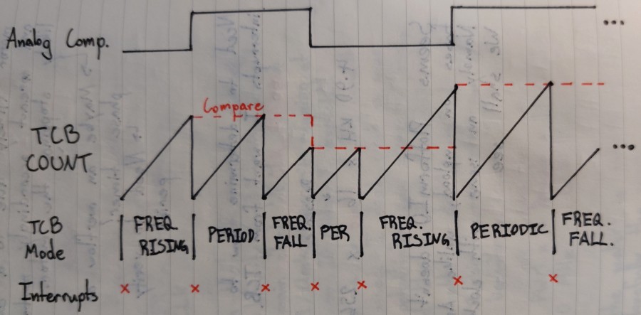
By constantly alternating between these two modes I should be reliably commutating the motor. I prepared a little chart to show how this should behave in theory.
Before I actually went to test this though, I decided to develop and test the buzzing feature.
Buzzing
The buzzing feature was largely unchanged from V2, except to make the pin assignments match the new board.
In testing this, I unfortunately fried my last two remaining MOSFET drivers for reasons that aren’t clear to me. My best hypothesis is that since I was raising the duration I was driving the motor during buzzing, I built up too much energy in the motor coils and the inductive flyback damaged them.
Without any more MOSFET drivers, my development and testing was stuck.
Outcome
Unlike with V2 there isn’t any clear progress I’ve made in my drone project overall with this version. I’ve just about managed to approach what I achieved with V2. I have no doubt in my mind that if I had more parts to spare I probably would have managed to control the speed of a BLDC motor with this revision, maybe even by now as I write this.
Who knows, hopefully V5 will get me over that line!