ESC V2
Table of Contents
Overview
This was my successful attempt at miniaturizing my previous ESC, from 65 by 35 mm to 40 by 25 mm. It is completely electronically identical to V1.
Unlike V1 I actually went ahead and not only built one proper, but developed and ran code on it. Eventually actually managing to properly spin a BLDC motor, albeit only at 100% due to hardware constraints of the microcontroller used.
Takeaways
- I needed a revised board that enables proper PWM control of the inverter
- New microcontroller
- New traces to suit the new microcontroller
- Record any hack-y tricks you need to pull or risk forgetting them! R.I.P. two boards. (See Chip Flip Section)
- There are lots of ways to accidentally fry your own board when working with mixed voltages. To name a few:
- Reversing polarity
- Driving pins on unpowered chips
- Shorting power rails
- Inductive flyback
- I need to fix the programming interface for ISP over SPI
Detailed Report
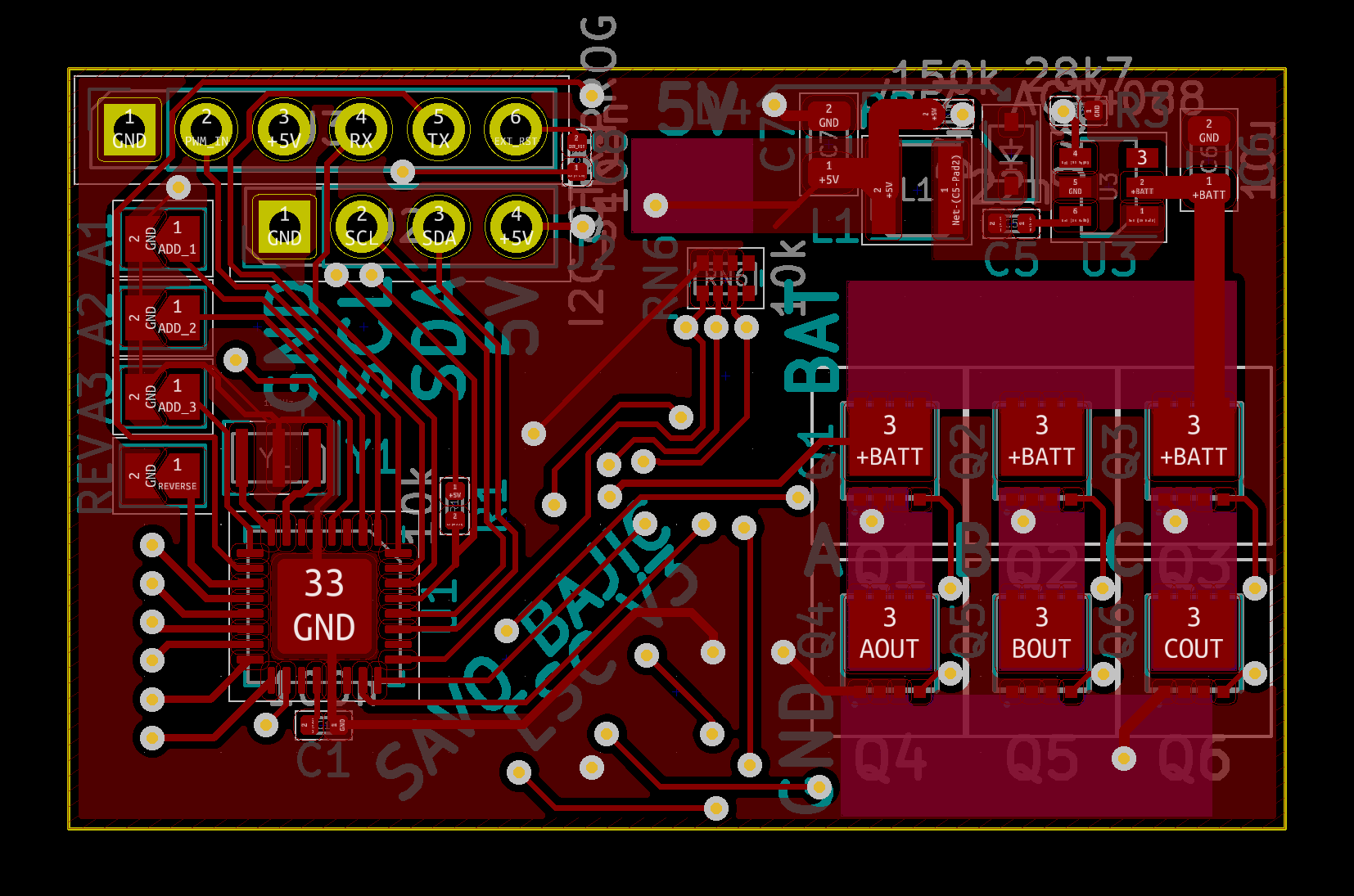
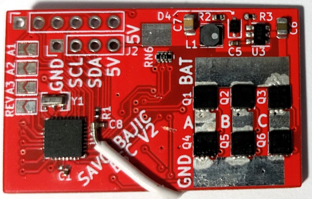
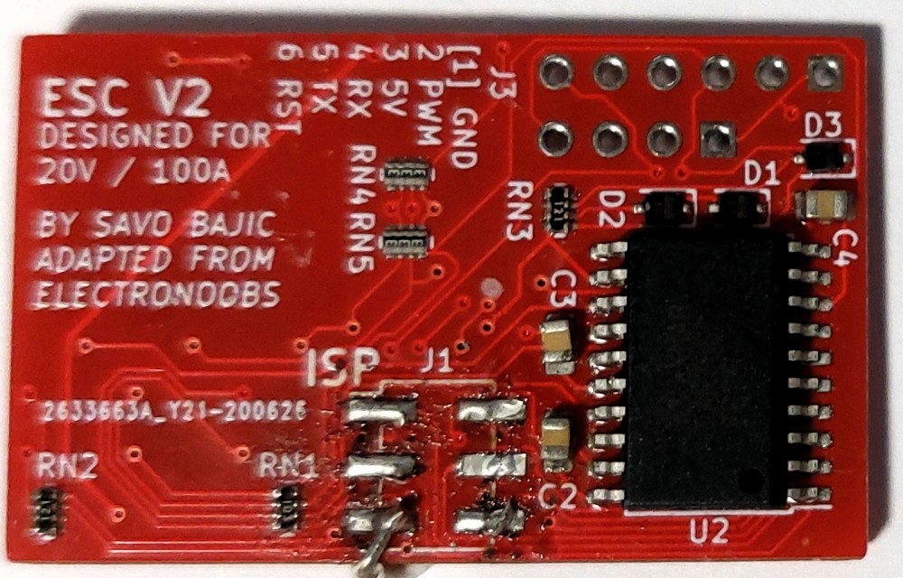
The goal of this revision was to miniaturize the previous version to something that would fit more easily into the drone’s frame. So although the circuit remains the same, the layout was completely redone from scratch, using more compact versions of components. The resulting board was 40 by 25 mm, down from 65 by 35 mm.
The boards were purchased and assembled so development could be done with them. The code is where I started to really deviate from the work of ELECTRONOOBS that I was following. I ended up rewriting much of his code to suit my system (I changed the purpose of some pins on the ATmega) and my desires (e.g. I2C). I then made significant alterations to his code to correct his handling of zero-crossings and commutations!
In the end I was able to achieve most of what I had set out to. I fell short of my goal to do proper speed control due to a lack of available hardware timers, some routing choices I made, and a shortage of parts (due to parts damaged during development).
Circuit Design
Since this is the basically the same as V1, please refer to its section on the circuit’s design. My only change is using the ATmega328PB in place of a ATmega328P, the PB is a direct upgrade for the P model so the connections and code can remain the same.

Note: there is a connection from the RST on the ISP header (pin 5 - J1) directly to RESET on the ATmega (pin 29 - U1) that was not present in V1 or V2. This was put in to reflect the bodge wire I needed to use so they would bypass C8 on the board, hence why this schematic is revision 2.1, not 2. (The appending letters change on U1 are just to designate package, it remains the same internally (ATmega328P)).
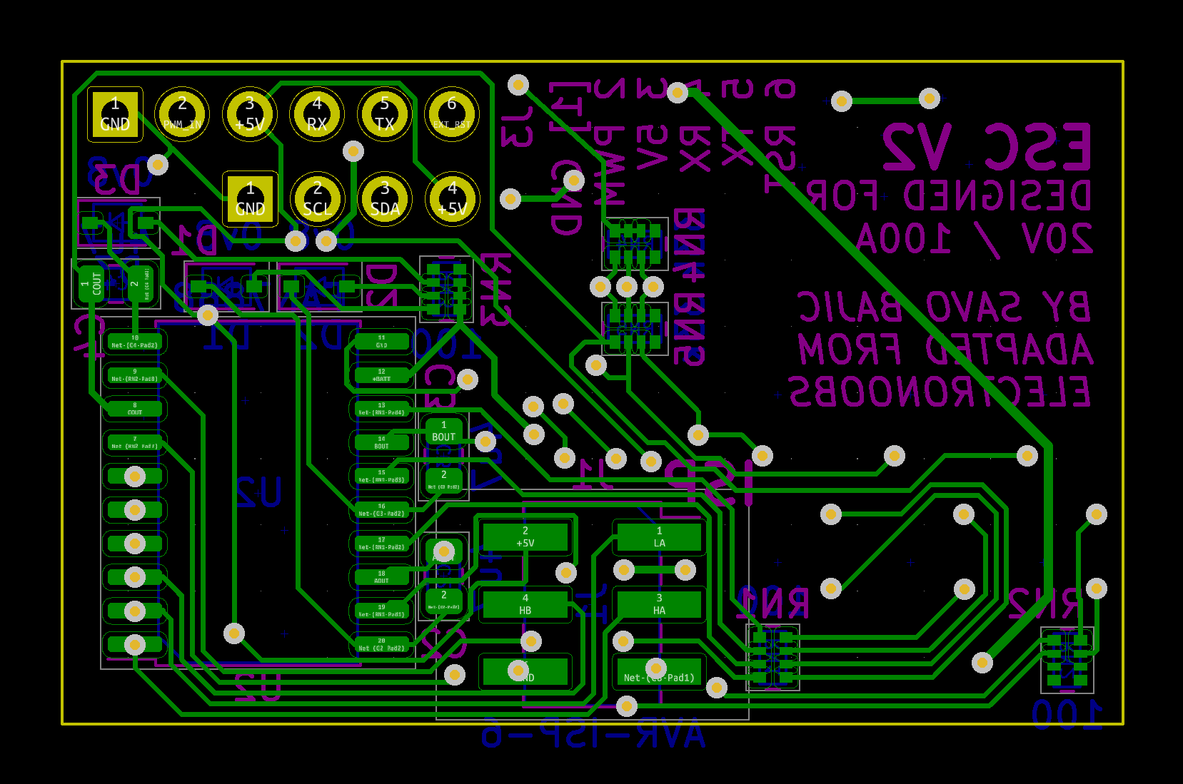
Layout
This is where the difference is made between the versions. To reduce the overall size of the board to 40 by 25 mm, I had to make several changes to the way I laid out the boards. I decided to no longer have all the inverter components on one side and the rest on the other, instead, I put components on a alternating sides based on their stage in the control cycle.
- Microcontroller (top)
- MOSFET driver (bottom)
- MOSFETs (top)
- BEMF resistor arrays (bottom)
In doing this I made it easier for me to make clean traces since most connections needed a via, and I could place these vias such that I could change the “order” of traces when changing layers which was needed on several occasions.
In addition to changing the organization of parts to make routing more manageable, I also changed some parts for equivalent, but smaller form factor versions. This was mainly done with the resistor networks, but I also changed the ATmega to use the QFN-32 package that is smaller (5 by 5 mm) than the TQFP-32 (7 by 7 mm).
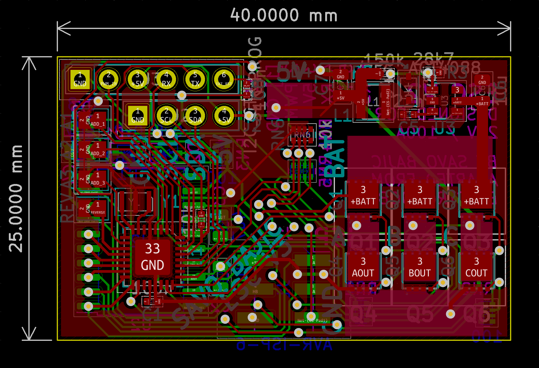
The bottom of the board housed the MOSFET driving circuitry and most of the resistor networks used for BEMF dividers. Since the AVR ISP header and the MOSFET driver share many connections I put that on this side as well.
In addition to the aforementioned microcontroller and MOSFETs, the 5 V regulator was also put on the top side in the top right corner of the board. Unlike the first version where I had a clear “input” and “output” end for power lines, I shortened the power rails to basically the bare minimum and will now be soldering the power supply wires closer to MOSFETs. Not only does this reduce space needed, but also resistive losses in the system.
Assembly
Assembly was a standard affair. Stencil, paste, place, reflow, flip, stencil, past, reflow, done. I should probably start making little slideshows.
There however was a hack(!) I had employed.
Flipped Chip Hack
A bit of context, I designed the boards early in the summer but didn’t order them until later in the summer with other projects I was working on at the time (to save on board shipping costs). Once I ordered the boards I went about looking to gather the components used on them. Unfortunately for me, after I committed the PCB order I found out that the voltage regulator IC I selected was out of stock everywhere and there were no pin-compatible replacements. I did however find a slew of ICs that had a mirrored pin arrangement (so I guess my chip was just trying to be special). So the idea dawned on me…
Why not just flip the ICs and bend their leads the other way? This way they would match pin assignments.
So I went ahead and ordered the parts to do exactly that. I unfortunately do not have any photographs of the flipped chips on boards. I do however have photographs of what happened when I forgot in the week between ordering parts and assembly, of this hack I was supposed to do.
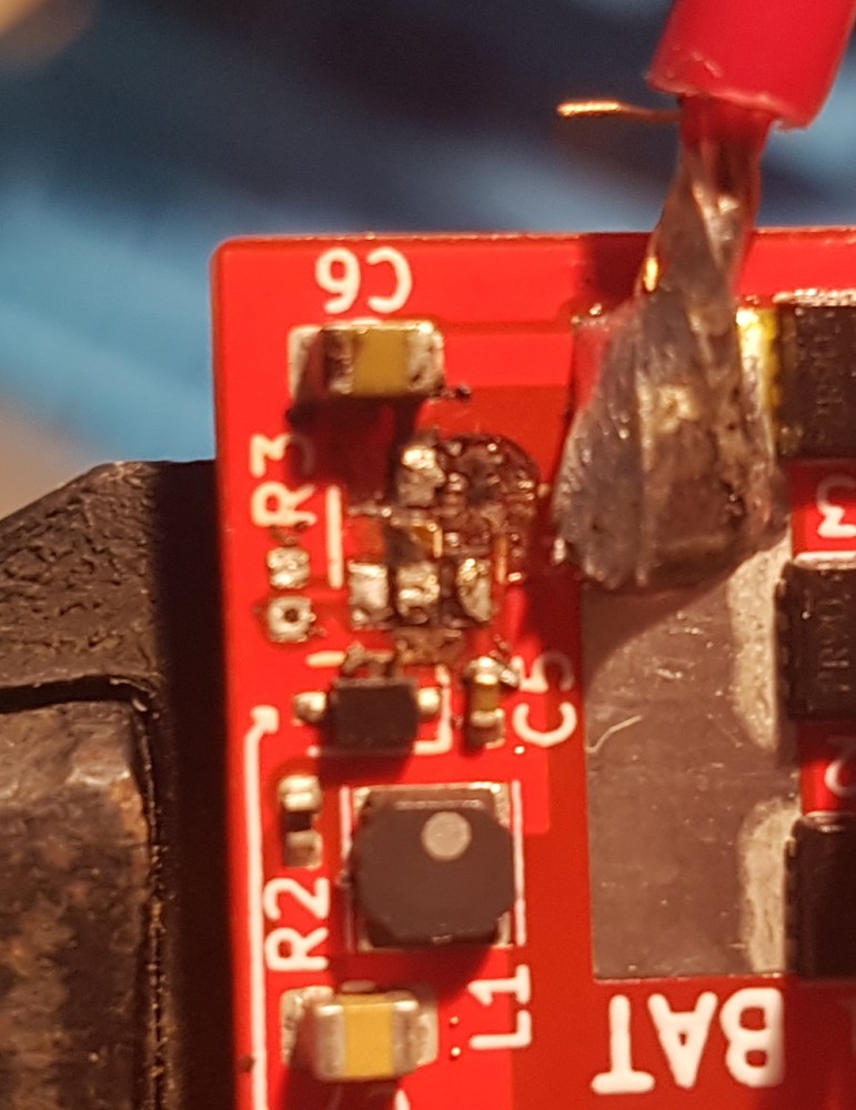
Having one IC literally explode when you turn on the power is shi-poor luck at the best of times, twice is a conspiracy! By not flipping the ICs they were being driven in all the wrong ways and the failures cascaded frying not only the regulator, but also all other ICs on the boards. It was only after the second one that I remembered what I was meant to do when installing them. A sour reminder to improve my documentation practices.
Testing
After assembly I wanted to do some basic functionality tests of my boards to verify they would work as I expected them to.
The first, and most basic, being the power on test. Simply apply power and see if any parts of the board are misbehaving or getting warm to touch. This was spectacularly failed by two boards as described in the chip flip section.
Once the boards passed the power test I would probe the power lines and outputs to verify that they were in the expected state. All boards that passed the power test, also passed this.
Uploading Code
The final tests I needed to do before I could really start developing for the ESCs was testing if they would accept code. This revealed some issues the design had, as well as some issues I did not experience before.
First off I had to burn the Arduino bootloader so I could develop programs using the IDE and upload them over serial to the ESC. This had to be done using SPI, for which I was using another Arduino as I have in previous projects. Since I was using an Arduino instead of a dedicated programmer with a buffered output that uses the target power (that I did not have at the time), I made use of it as a both a programmer and the power source during programming instead of supplying the ESC with a “battery” voltage.
This approach ended up costing me a MOSFET driver chip because although I was supplying power to the microcontroller, there was no supplied power to the driver. Thus when the pins used for both programming and controlling the driver were driven high, this high was several volts over the “supplied” voltage to the driver and caused it to fry.
Thinking I had solved the issue I disconnected the 5 V connection from my Arduino to the ESC, powered it properly so it was running off its own 5 V supply and tried reprogramming it again. Somehow at this point, I assume due to the mismatch of “5 V” supplies, I had fried a microcontroller.
New Commandments, New System

Frustrated with issues, I wrote down some “New ESC Commandments”. These were pointers that I would use going forward to avoid the same mistakes when working on this revision and what to address with future ones.
- Removing the 5 V regulator. The drone will have a central one that will also be specifically designed to remove noise from motor operation
- Add LEDs for status of power lines and general use
- Supply battery voltage before connecting programmer
- Try to use separate pins for programming and driver control
Since I ran out of ATmega328PBs, I decided to continue working on this revision I would revert to using an ATmega328P. I would do this by removing the PB from a board and soldering wires between the Arduino Nano to the ESC board. This required me to solder 11 individual connections:
- 1 common ground
- 6 MOSFET driver control signals (three phases, high and low for each). Soldered directly to the IC leads.
- 3 divided BEMF voltages (resistors soldered to ESC)
- 1 divided “zero” voltage (resistors soldered to the previous resistors, basically hanging in the air)
The completed system made good use of my new helping hands to ensure everything stayed together.
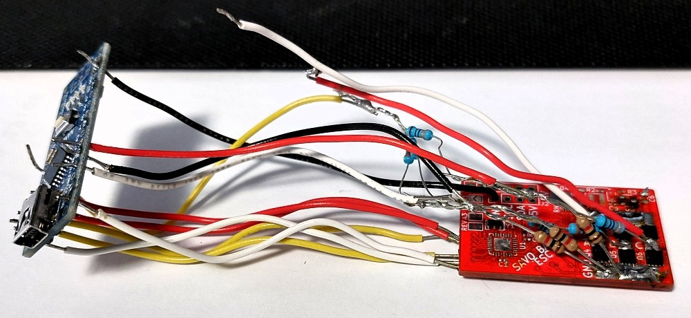
Testing on the system was continued in parallel with firmware development, using this Arduino-ESC system in place of a proper ESC V2. Although its hardware was more limiting than the ATmega328PB I originally intended to use, it wasn’t critically limiting. Using the Arduino board brought the advantage of a much simpler development experience, as long as I was careful not to break any of the connecting wires.
Motor Testing
I avoided having a motor installed in the system to be driven until I was comfortable with it because I didn’t want to potentially stall the motor with bad commutations and damage something, either with excessive current or from transient spikes as I was working on unrelated code. So I either ran the ESC unloaded initially, or I would simulate the load with high value resistors as needed.
For example, I used an oscilloscope to monitor the (unloaded) output of inverter phases to see that I was stepping through the commutation cycle correctly. When it came to testing the zero-point crossing detection, I used potentiometers to manually swing the voltages.
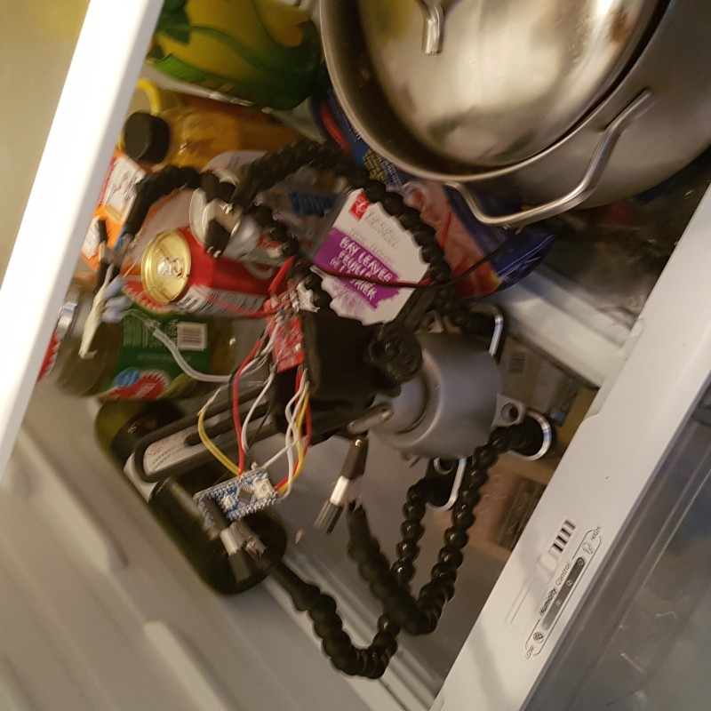
Once it came to the point I needed to actually test with a motor, I decided to start with a smaller, inexpensive (free) motor than the ones I purchased and intended to actually use in the drone. The motor I used for my tests was salvaged from an old floppy disk drive which I soldered power resistors to. These resistors not only acted as a convenient contacts for each phase but also as a way to decrease the potential stall current of the system. The power resistors and the windings of the motor sum to roughly 3.8 Ω of resistance for any given stage of the commutation cycle, so when running at the nominal 12 V, the system would stall with roughly 3 A which all components could sustain for extended periods of time.
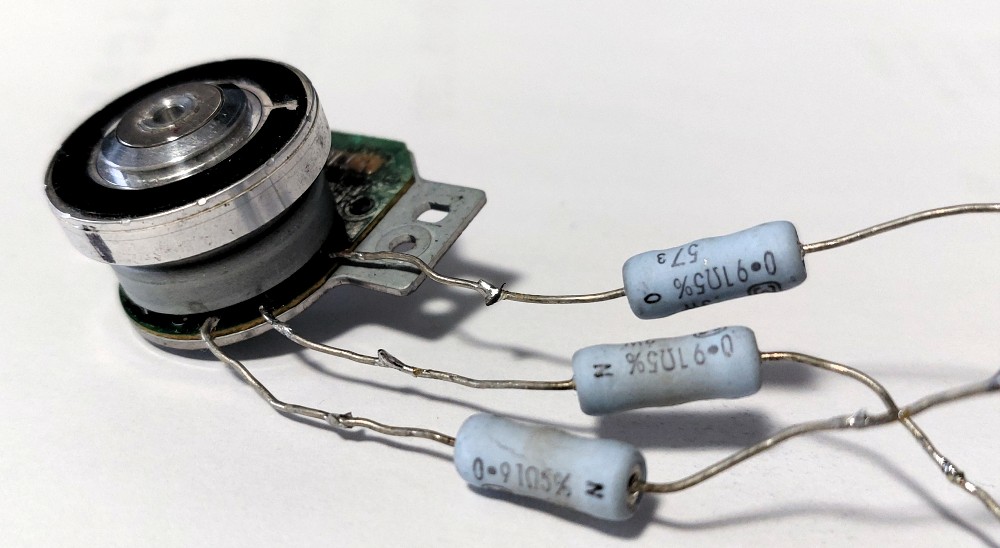
The browning in the middle of the power resistors are indeed burns from continued use from tests I was doing above the usual 12 V. I also added wires to bypass the resistors when I wanted to do full power tests, I removed these for the figure above, but the solder joints bracketing the resistor when they were are visible.
Fun little tidbit: During motor tests, especially at at the beginning when the motor was stalling a lot I would move my system to the fridge to cool quicker so I could continue testing. No, condensation was not an issue.
Developing Firmware
The firmware on the ESC was developed using the Arduino IDE and written in C. I wanted to prepare and be sure of as much as I could with non-motor related features first since they were easier to test and would allow me to be prepared for the real deal of working with the motor and the issues it could cause.
I had a rough order for the features I was going to try implementing:
- Implement software PWM
- BEMF detection (zero-point crossing handling)
- Commutation
- I2C communication/control
- Buzzing on the motor
- Running the motor
Software PWM
Due to my selection of pins, I was forced to use software PWM if I wanted any PWM on all the MOSFET outputs. I could have gotten away with just using hardware PWM on the high-side pins like ELECTRONOOB did, however due to my pin arrangement I did not have all the high sides on PWM either. So since I was going to have to do it on a few, I was going to go all the way to keep all of them synchronized.
To implement software PWM I used a periodic interrupt using timer/clock 1. During this interrupt I would either set the pins to the required output for the “on” period, or reset them all to zero for the “off” period.
I wanted to implement phase correct PWM, where the duty is centred in the period. This is generally recommended for motor (or other reactive load) control compared to the standard “quick” PWM where the centre of the “on” portion shifts with duty. The reason being that all outputs at the same frequency will remain in phase even if they have varying duties. This is not particularly relevant for this project since all phases are going to be operating at the same duties, but I believed it was something neat to try.
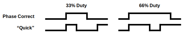
I did get this to work, although I had to do some tricks. When doing periodic software interrupts on the ATmega328P, one can only use them in what would basically be “quick” PWM mode, with an interrupt available partway through the cycle and another as the clock resets. To get my “phase correct” method to work I used the interrupt partway to change the output states, and the reset interrupt to set the the interrupt point to keep the waveform centred across two cycles.
The results of this were decent, although as I pushed for a higher frequency (above 8kHz) duties at either extreme were unstable as the software would take longer to run than the period to actually reach the changes. This basically meant that I had to clamp duty to an extreme when they were within 15% of either end, effectively reducing me to only 70% controllable speed range.
These issues only got worse however when BEMF interrupts were introduced, as their interrupts would get in the way of one another.These constant interrupt races are the reason the motor speed cannot be properly regulated.
BEMF Monitoring
Testing and implementing the analog comparator interrupts for the microcontroller was relatively straight forward and I was able to reuse much of ELECTRONOOB’s framework for this part. I simply had to set an interrupt for the comparator like I did with the timers for PWM, then to select the pins to compare as well as which edge to trigger on needed me to adjust two registers.
I tested my code for this to great success with some potentiometers as mention in the testing section.
Commutation
This is where I spent a good portion of my time, as I needed to reteach myself and reassure myself what I was doing was right in terms of BLDC control. The reason I had developed doubt was because when I was looking at ELECTRONOOB’s code for this, he would commutate his motor right after passing the zero-crossing, however if we look back at the theory of BLDC commutation one can see that zero-crossing is halfway in the step, thus the system needs to wait another half-step before it commutates. At high speeds this half step would be roughly 100 to 300 microseconds.
ELECTRONOOBS seems to have dodged this due to his use of a for loop in the interrupt that checks 10 times every 10 us if the zero has been indeed crossed which leaves a delay of 100 us which in combination with other factors related to code execution probably generates a delay of between 150 us and 200 us between zero-crossing and commutation, which is tolerable in most circumstances.
I wanted to approach this in a more proper way, using an additional counter/timer. At the start of each commutation step it would be reset and start counting up. Once the zero crossing was reached, the counter’s value would be doubled to estimate the exact time to commutate. Once the counter reached this threshold a software interrupt would execute to commutate the motor, resetting this recycle.
This worked well in isolated unit testing, however when combined with the PWM interrupts, their constant racing would lead to the system failing to properly drive a motor.
I2C
Getting I2C up and running was easy thanks to working in the Arduino framework where there is well documented examples for these sorts of applications where a device is configured to respond to commands from a central dispatch. To exchange data back and forth I opted for a set of “virtual I2C” registers on the ESC, similar to how many I2C devices are communicated with. The central controller addresses the target, and provides the index of the register it wants to either read or write to. Then the central provides the data it wants to write in the same exchange, or it starts a request to withdraw the data.
This was tested using a second Arduino connected to the one on the ESC and worked without issue.
Buzzes
Getting buzzing to work wasn’t too difficult, I was able to reuse most of ELECTRONOOB’s concepts. I wrote my own functions from scratch since I didn’t like the way he structured his code. The basis of buzzing is just powering a step for a brief period of time, and the powering another step. Alternating between them at the desired frequency for your buzz.
Testing was done with the motor attached. During testing I had to tinker with the periods a bit to balance an audible buzz with not frying the system because I am intentionally stalling the motor.
Success!
I managed to achieve all the baseline supporting features I needed and they passed my tests, such as I2C data exchange and motor buzzing. I eventually got the motor to spin up and then sustain rotation at full speed for extended period of time. Below I have a video of the ESC spinning up a motor and having it run for 10 seconds.
… Well Kinda
The ESC works perfectly, if you want the motor on at full power. However any attempt to moderate the power with the software PWM implementation is quickly met with failure as the interrupts for commutation and “PWM” start to collide and the motor seizes up.