Hardware Clock
Table of Contents
Overview
I have for a while wanted to take a break from microcontroller-based projects and try my hand at doing a project without one. Without completely surrendering myself to the world of analog, I took a stop towards this by try to do the classic hobbyist project of a clock, but only with discrete logic chips.
The idea came to me when browsing through a cache of old electronics a friend of mine had come into and a friend mentioned they wanted to learn to make a clock with a microcontroller so I decided to make one of my own too.
Currently I have produced the modules, and verified they work at a basic level in unit testing. However, when put together they don’t work correctly. There is an issue where the counters are counting more than the should that I am currently trying to find a solution for.
Requirements
- Show the time in some format
- Be modular by function
- No microcontrollers allowed!
Objectives
- Be accurate to within two seconds a day
Takeaways
- I’m a bit rusty at breadboard prototyping, need to double check my connections are actually working as they appear they should with continuity tests.
- Discrete logic isn’t as troublesome as I expected, but this also is a basic project really. I would look to maybe use some in future projects, especially for safety systems and such.
- Does h4x0r aesthetic == poor user experience?
- Specify the location for the fabricator to put their order number on the board, especially if aesthetics are a factor!
- Electromagnetic Interference can be funky to spot
- Decoupling capacitors are needed on for all ICs and in all circuits regardless of complexity/speed!
Detailed Report
I’ve wanted to do something without a microcontroller for a while now since that’s been the common denominator in basically any project of moderate scale I’ve undertaken thus far. During a visit back home I was invited by friend to check out a cache of second-hand electronic components he had purchased to see if there was anything that tickled my fancy.
These were a collection of organizers chock-full of goodies, from bulky switches and potentiometers down to individual passives clearly pried from some long forgotten control cabinet. Among these dozen or so cabinets were a few stuffed with logic ICs from all the standard families: 7400-, 4000-, or 4500-series classic.
Initially I was just grabbing ones that looked cool to potentially use in some future project. However my other friend mentioned they wanted to make a clock so I took their idea and ran with it, grabbing ICs I felt would be useful for the job and a fistful of LED displays.
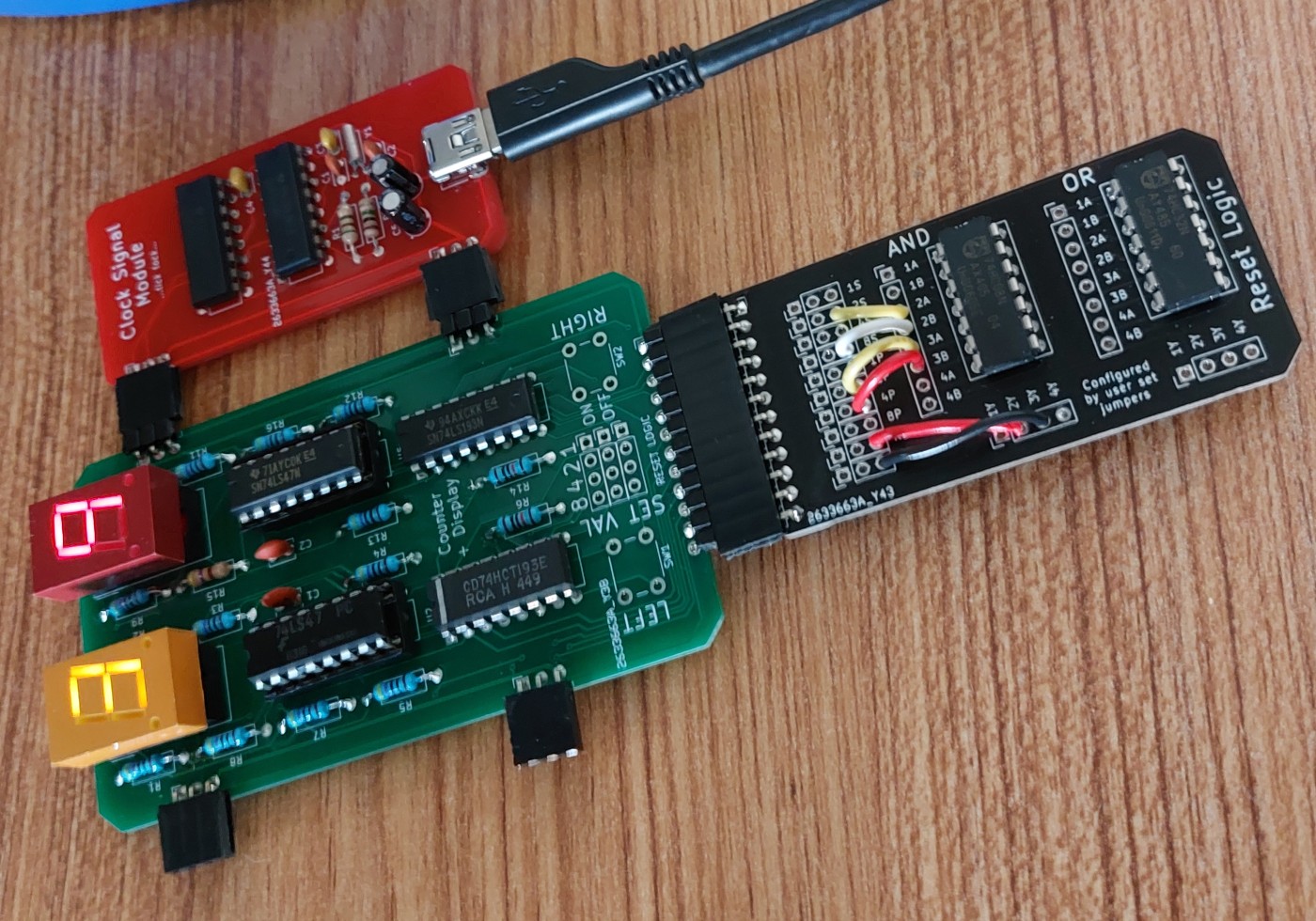
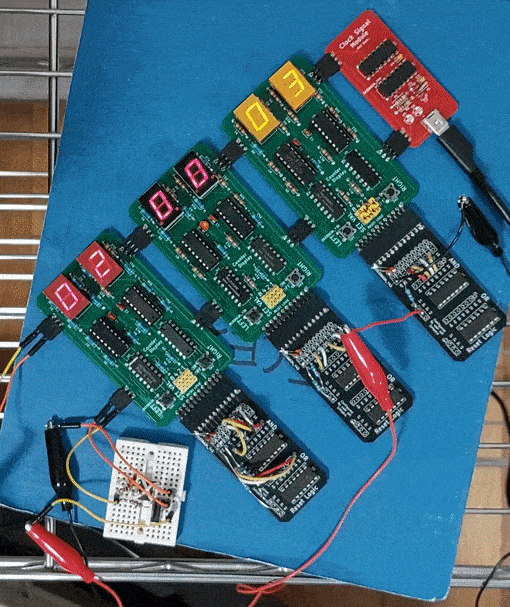
I quickly realized that this circuit was going to have to be large to fit all the ICs, especially since they all came in DIP14/16 packaging. So I felt that a modular design would be wise to keep things (and issues) separate. It would also help create a sort of cliché “80’s hacker” aesthetic when paired with all through hole components and floating jumpers.
Module Design and Prototyping
I broke the system into modules based on function:
- Displays and counters. Two digits per panel
- Reset (rollover, carry) logic for each digit
- Base clock signal and power delivery
Chip Choice
Limiting myself to the chips available in the cache, I selected the following chips for the different modules:
- Display drivers (they share functionality pin-for-pin for easy switching as needed)
- 74LS47 for common anode displays
- CD4511 for common cathode displays
- Counters
- 74LS193 programmable 4-bit counters
- Reset logic
- 74LS32 quad OR gate
- 74LS08 quad AND gate
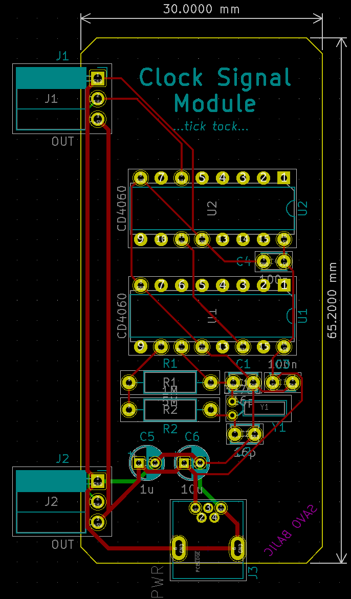
- Clock divider (for 32.768 kHz crystal to 1 Hz base)
- CD4060
Displays
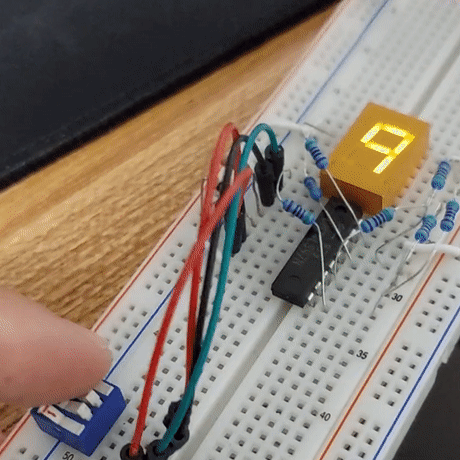
The first part I worked on prototyping and getting working was the displays since they would be used to debug the rest of the circuit. Once I had sorted the displays based on whether they were common anode or cathode, I began to connect them to the drivers and would cycle through values to display using a set of switches to ensure I had everything connected properly. This worked without a hitch.
Counters
A clock is basically one large counter composed of individual counters for each digit. The ones on the seconds count to 10, then reset and increment the next digit, up to 6. At that point the minutes increment up, so on and so forth. Thus each digit needs its own counter in addition to a driver. These counters would count the leading edges of an input wave and output their value on four pins.
Reset Logic
The counters I used (74LS193) are true 4-bit counters so they rollover and reset at 16, so all digits need external logic to properly reset the counters and increment the next digit. To achieve this I am using some AND and OR gates to check the output of the counters and then use the result of this logic to reset and increment counters.
For example, if we want to rollover a digit at 10, we can use a single AND gate to see if the 8 and 2 bits are both set and then use it to reset the counter. This works because under normal operation the numbers increment upwards from 0 so there is no chance for the clock to overshoot and miss the reset. However if the user inputs a value over the set point, i.e. 11, then depending on the logic used, the system might not recent properly. I believe this is an acceptable error case because it will correct itself once the digit is reset, although it will through off the time in the process.
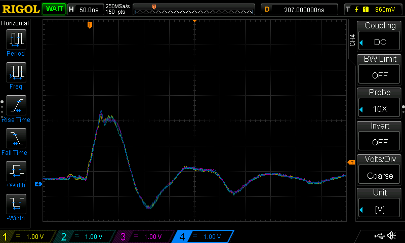
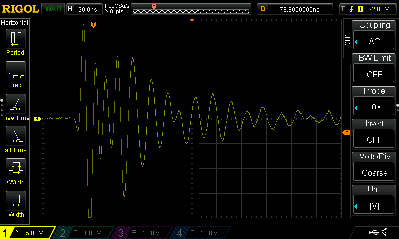
Below is a demonstration of a counter set up as described to count to 10 using the external AND gate.
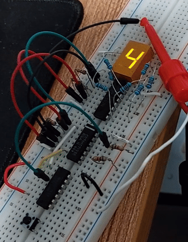
To ensure the pulse generated to reset a counter is long enough to also increment the adjacent counter I performed tests on cascaded timers that were successful.
Signal Generator
The heartbeat of the clock is a steady, accurate 1 Hz square wave. This square wave is generated using the same system used in most digital watches and real-time clocks (RTCs), dividing a 32 768 Hz signal down to 1 Hz. This is done by using a chain of T flip-flops that each half the frequency fed into them. 15 of these are needed to divide the 32 768 Hz (2^15) down to 1 Hz.
The CD4060 was designed for this job, having a string of T flip flops needed to divide the signal, as well as the circuitry needed to drive the reference crystal used to provide the 32 768 Hz. The only issue is that it has only 14 flip flops internally, so two CD4060s are needed to divide the signal all the way down to 1 Hz.
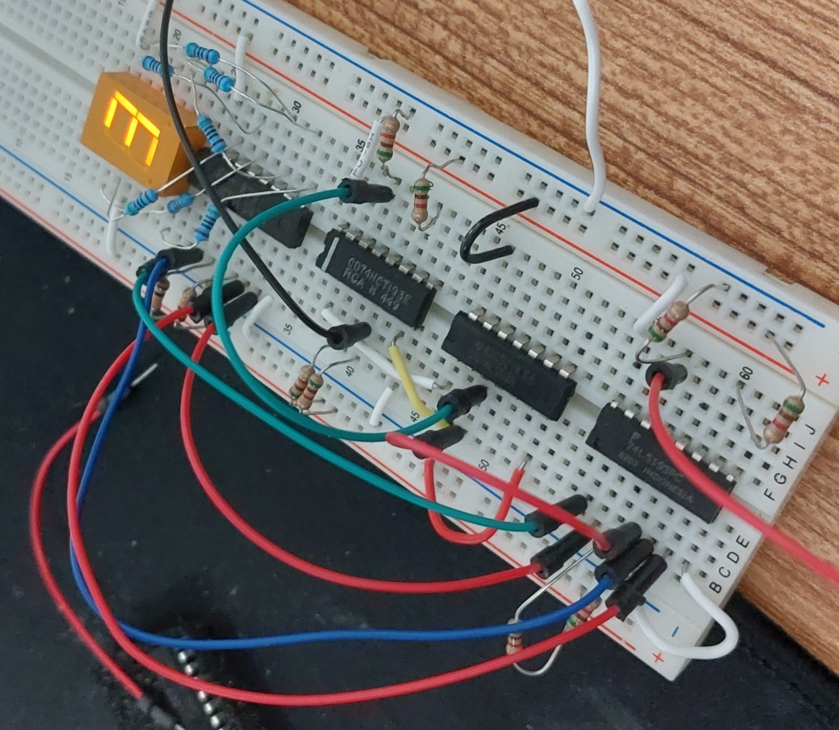
Prototyping Issues
Making the prototype module for the clock on a breadboard was where I lost most of my time. I was using a reference design I found and the system would work fine, however if I left it running for a few minutes it would start to shift its frequency higher until it would eventually just stop working entirely. This is not something I wanted. I wanted to make a “clock” clock, not an egg timer.
So I spent a few days trying to tune and dial in the values of the passives around the crystal, changing the crystal, even the CD4060 with brand new ones to see what I could do to improve the stability. The best I got was just about 3 minutes before failure.
In the end what turned out to be the cause of my issues is that the CD4060 did not have its reset pin properly grounded so it collected a charge during operation and resulted in these intermittent resets of the chip. This was caused by a break internal to the jumper I was using to ground it, inside the plastic head at one end.
Schematics
After prototyping I transcribed my work on the bread boards to proper schematics for each module so I could advance to making the circuit boards. I’ll explain them starting from the simpliest.
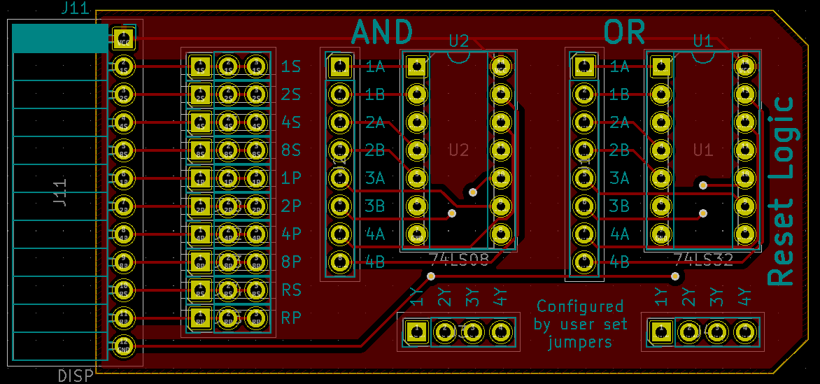
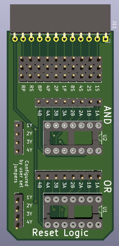
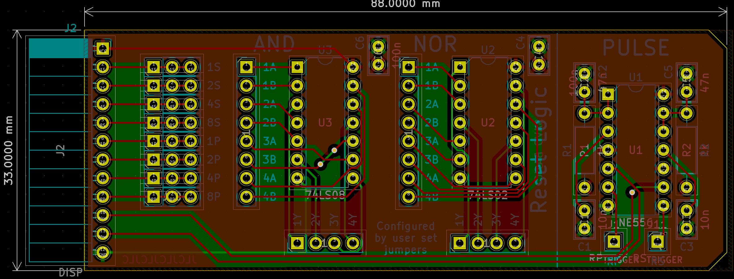
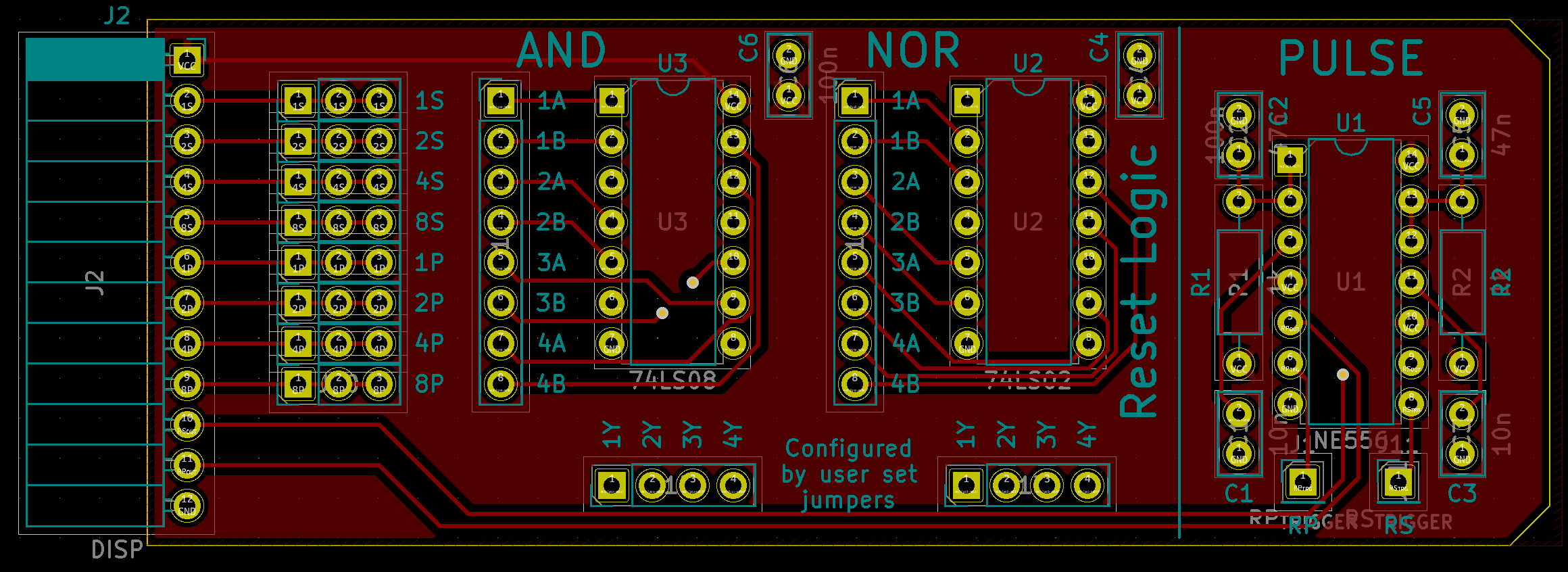
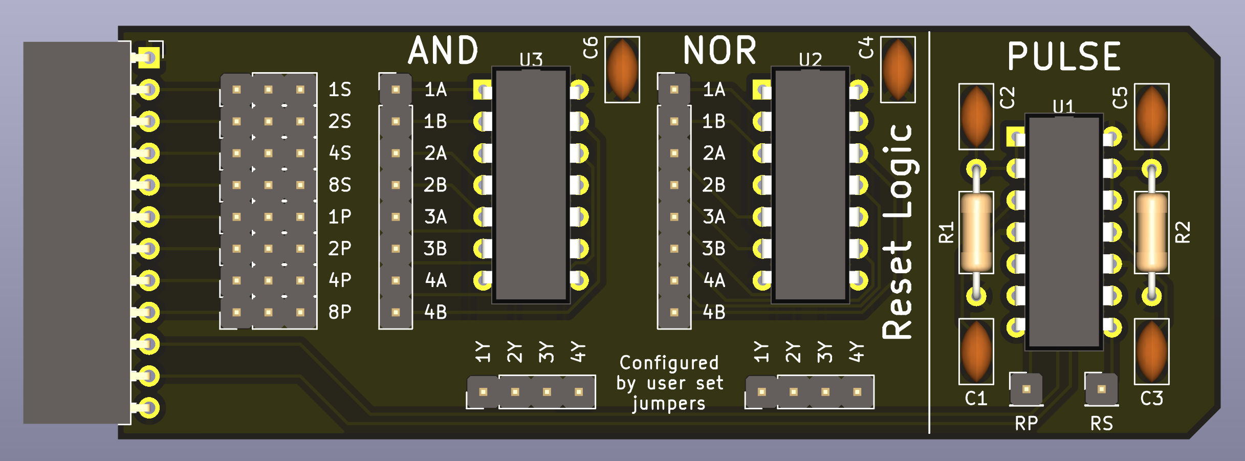
Reset Module Circuit
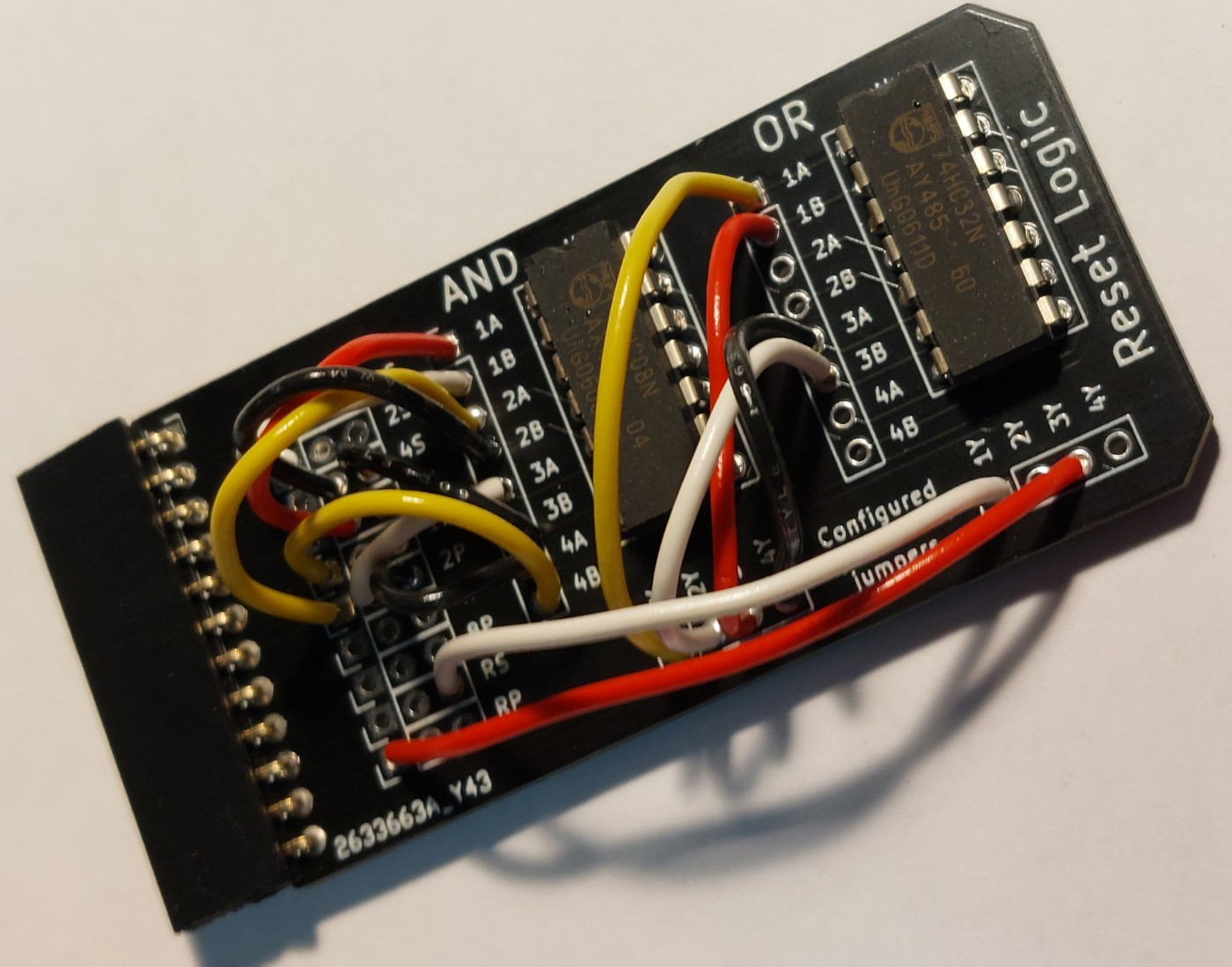
This one is just a a collection of headers for each signal and breakouts for a set of four AND and four OR gates. It is down to the user (me, for now) to wire the connections as needed for each reset signal they want as part of assembly with jumper wires.

For resetting/rolling over at 6 and 10, just one AND gate is needed, to do the rollover for hours (either 12 or 24 hour configuration) is a whole other monster, but can be done with the logic gates available.
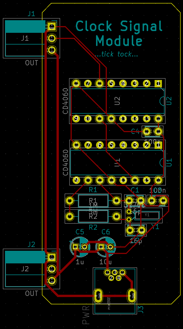
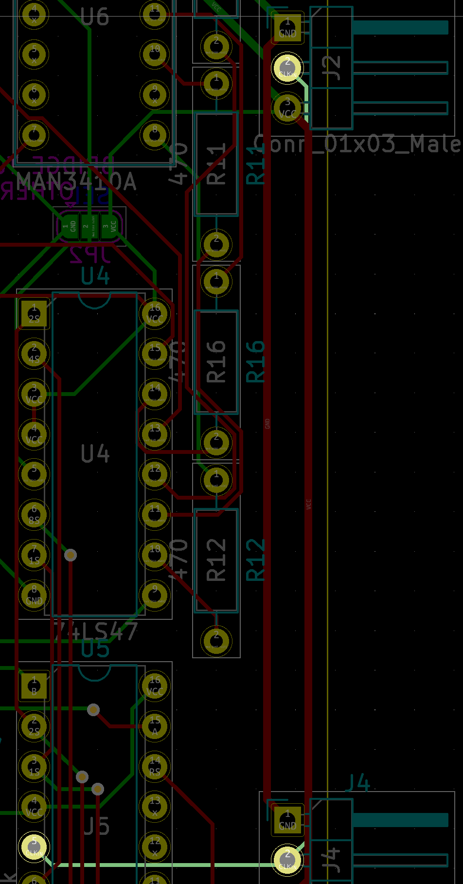
Signal Generator Circuit
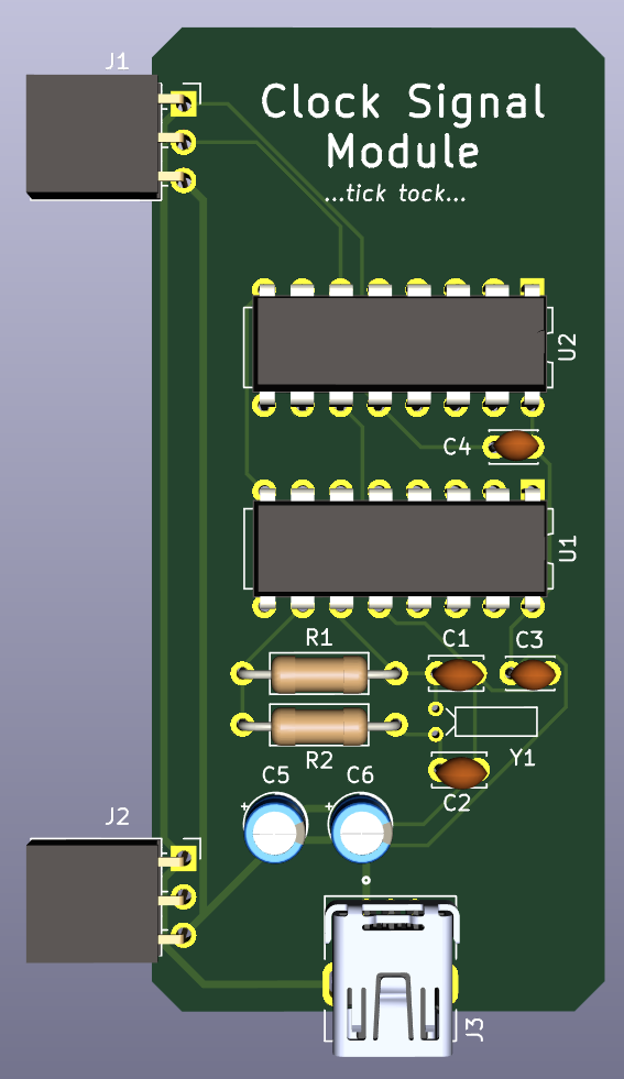
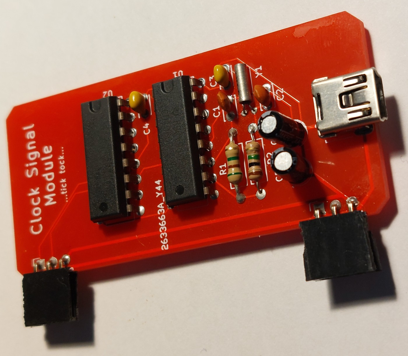
The signal generator is little more than two cascaded CD4060 chips to divide down the reference 32.768 kHz crystal signal. Since it is also the power source for the rest of the system, it has a USB connector and some capacitors to help smooth the power received for the system.

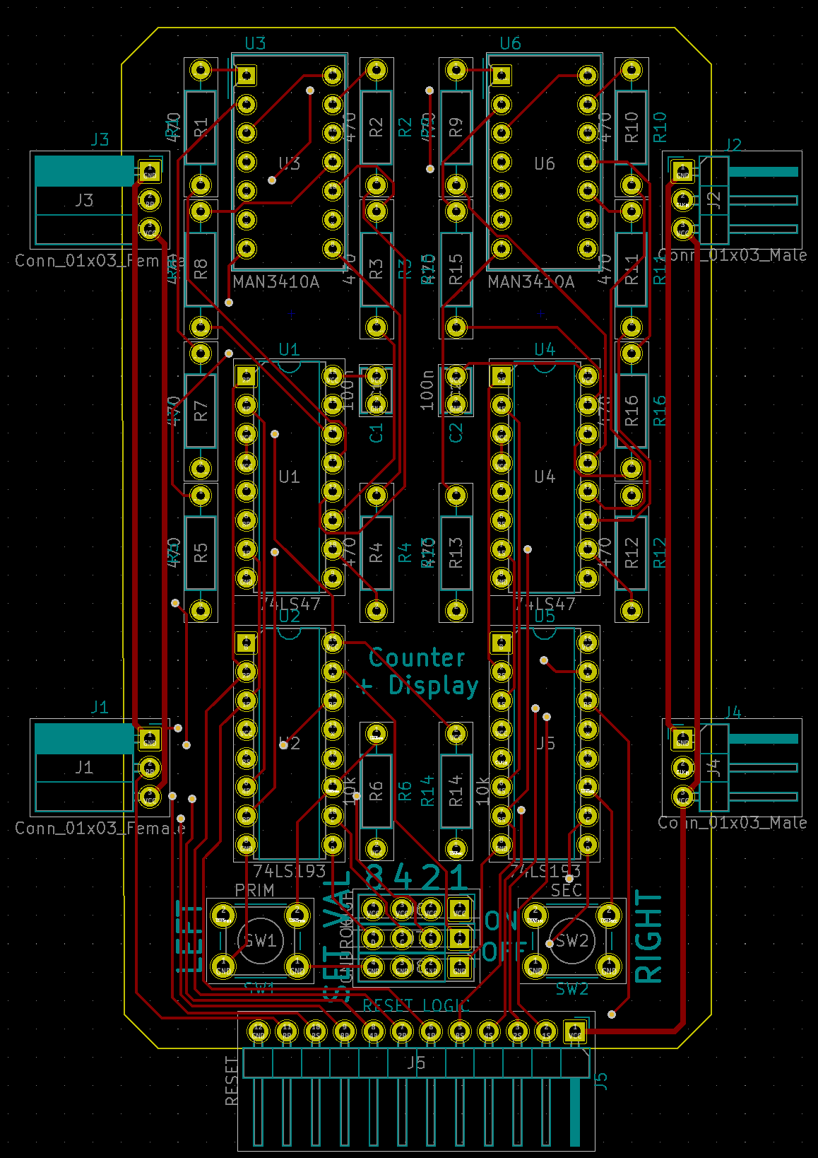
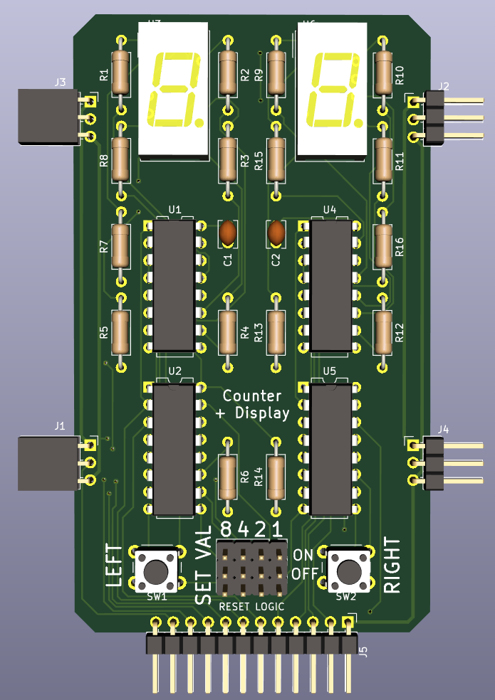
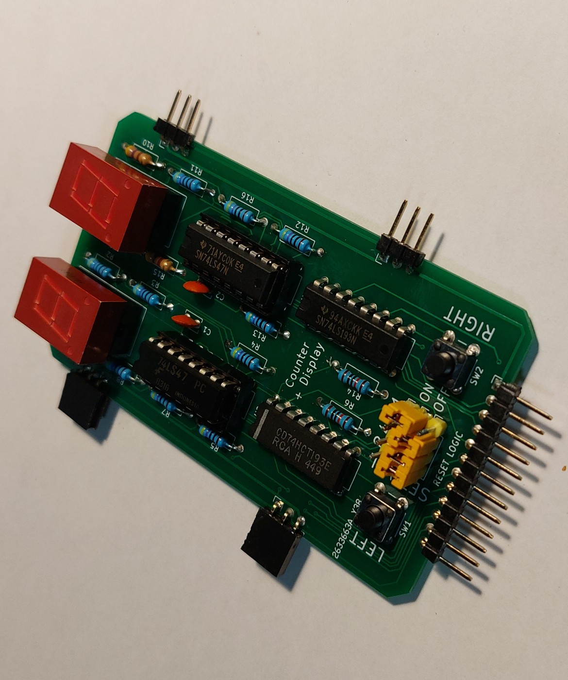
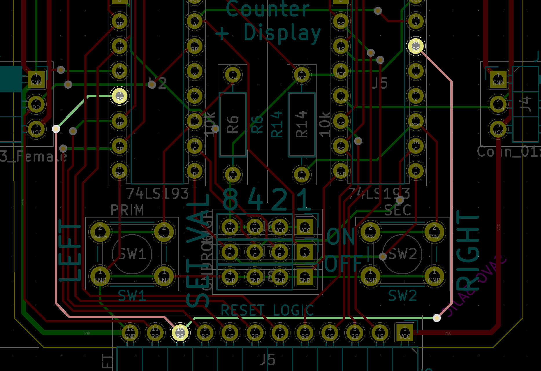
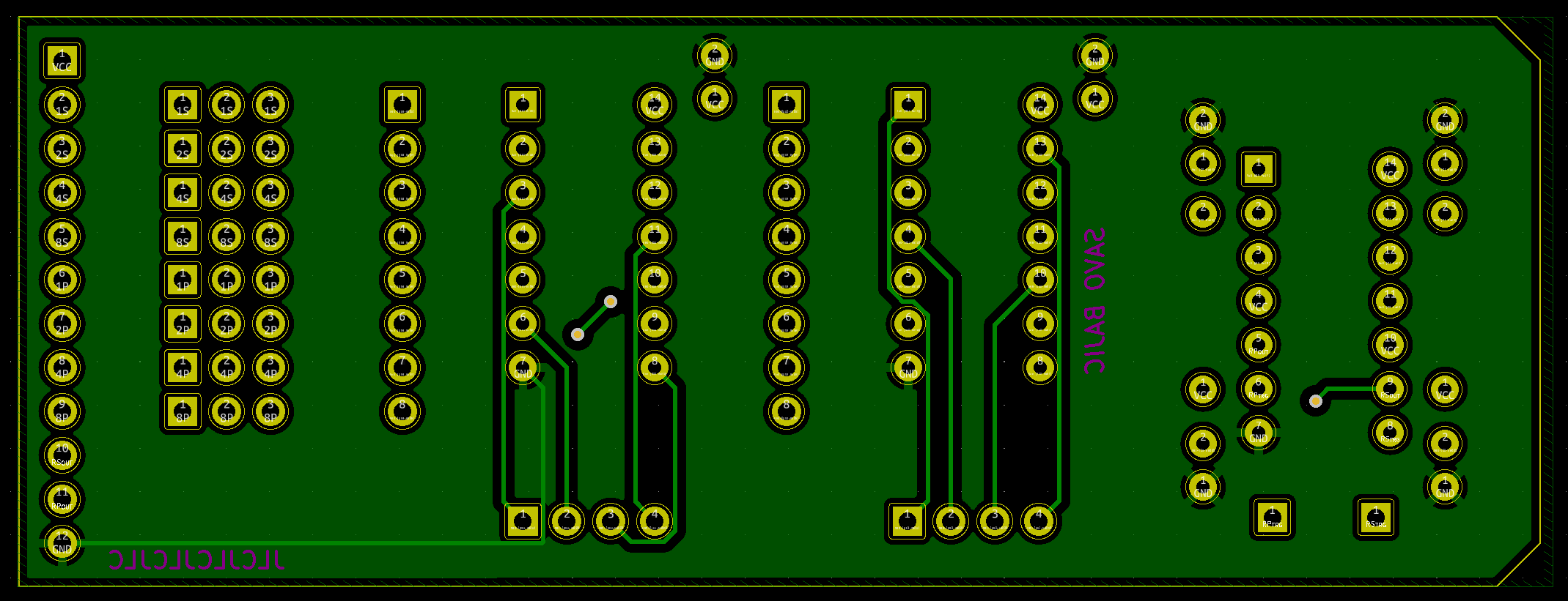
Display Module Circuit
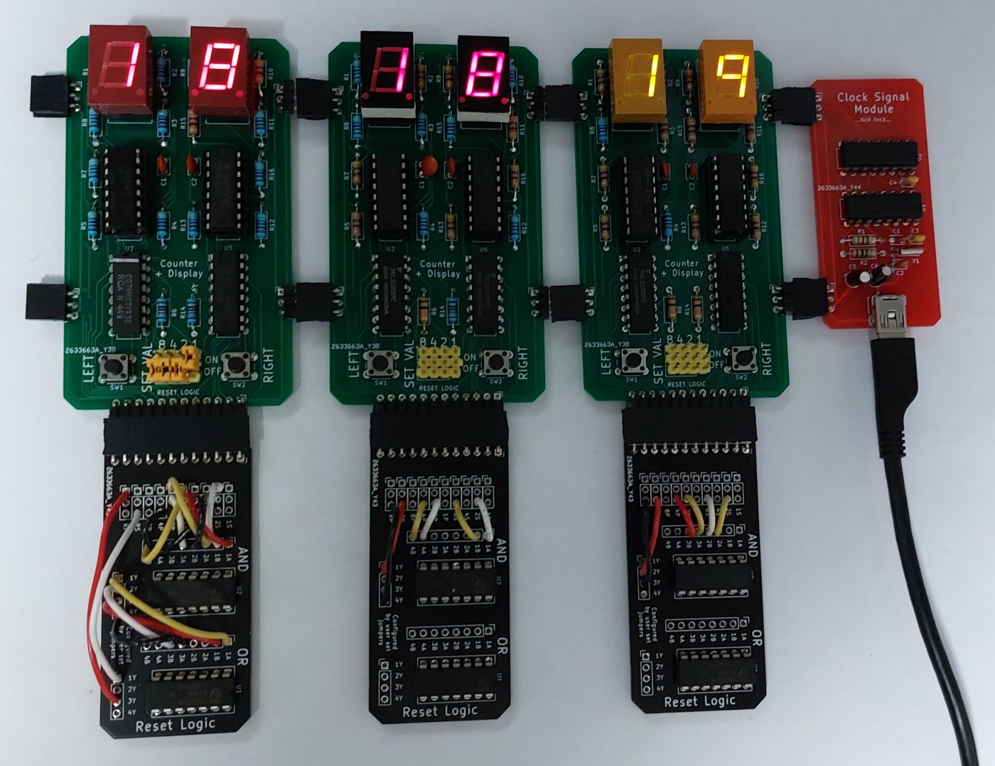
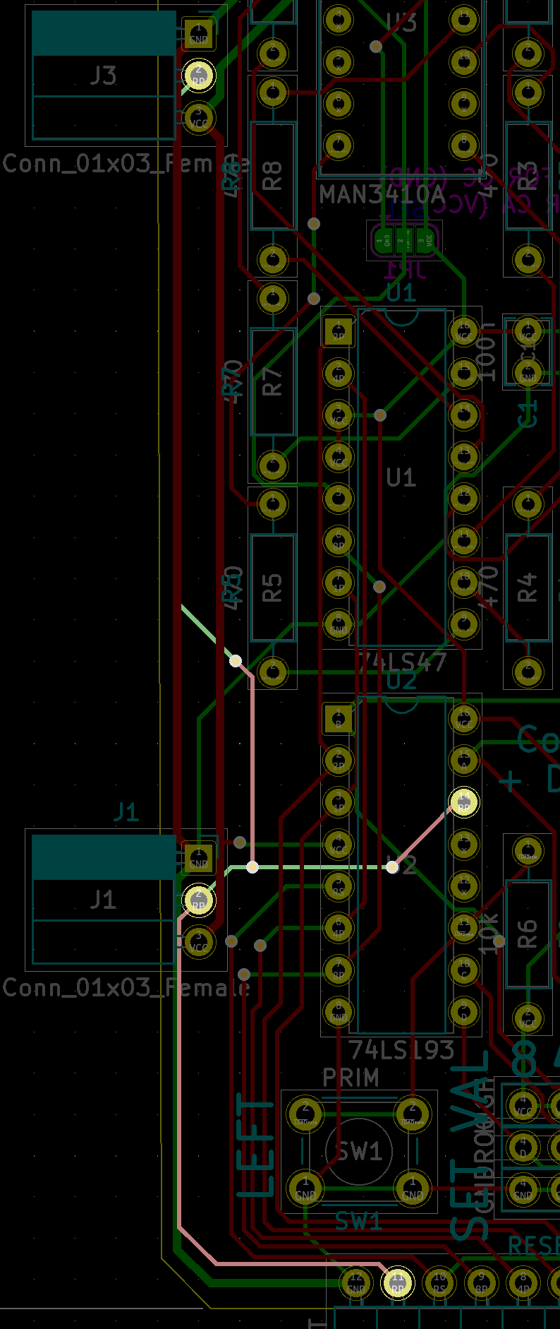
By far the most complicated module of the bunch, the display modules house two parallel counter/display systems each. The left (leading) digit is the primary, the right (trailing) digit is referred to as the secondary.
The basis of each is the counter, a 74LS193 IC, which counts the number of incoming pulses to it and outputs a four bit value (0 to 15 inclusive). These automatically roll-over (reset) at 16, but can be manually reset sooner. These manual resets are used to trigger a reset for the desired digit value, e.g. when it reaches 6 or 10 using the external logic chips which receive and return signals via the reset header. The reset of the secondary digit is used as the input clock for the primary digit, the reset for the primary is passed forward.
I added the ability for the user to set the digits using jumpers to set a value, and then pressing a button to load it into the desired counter. Originally I intended to use a more conventional and user-friendly button to increment counters but the issue of debouncing and safely combining clock signals would have needed me to add much hardware to the boards. On the plus side, I think the exposed headers will add to the “hacker” aesthetic when laid out.
The count from the counters is fed into the display driver ICs which decode them to drive seven segment LED displays. The displays I use are standard industrial ones that fit into the DIP-14 footprint. The digits come in two formats, either common anode or common cathode (CA and CC respectively), based on how their LEDs are tied together. This determines how they are driven so the driving IC has to be correct. For CA digits I use the 74LS47, for CC displays I use CD4511s. I chose these two since they share they can be placed interchangeably due to their identical pin allocations and input behaviour. The only functional difference between the two for me is how they handle the ripple blanking input (RBI) on pin 5. Fortunately the level this needs to be pulled to for each matches the common power level needed for their displays so I set it using a single solder jumper.

Layout
With my schematics wrapped up, I began the layout of each module. I used edge connectors to pass the signals between them since it will provide more structural stiffness compared to wire jumpers when hung up on a wall as well as result in a more compact assembly overall. A purely aesthetic choice I made was to use exclusively through hole components, this is really evident on the display board with all the resistors used for the LEDs.
The edge connectors between display boards and the signal generator are spaced 50 mm apart.
Looking back, one thing I regret is not specifying to my board house where to put their order numbers on my boards since they ended up just slapping it wherever it fit on the front(!) face of all my modules. Come on…
Reset Module Layout
The reset module is little more than a breakout for the two available logic ICs and the data signals from the counters. As mentioned before, it is meant to be wired at assembly to produce the reset when needed so I tried to make it reasonably easy to access and identify all the headers by hand without documentation.
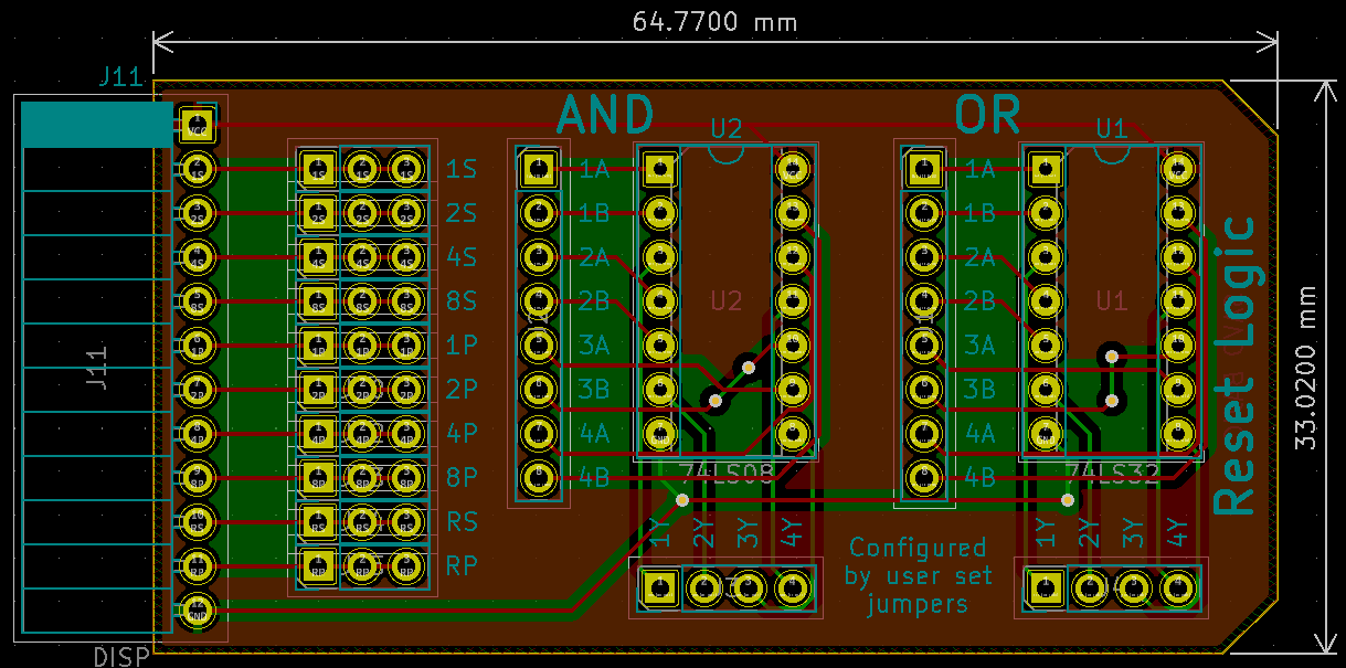
To aid the end user in wiring the reset logic I labelled all the headers with their signal names on the silkscreen for the top.
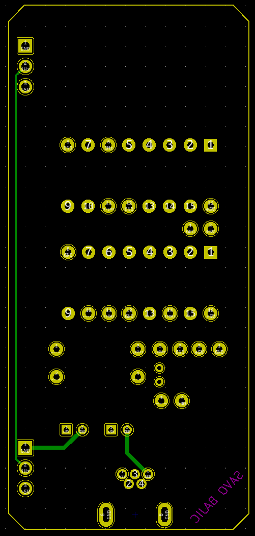
Signal Generator Layout
Not much to really say about this one, pretty simple layout for a pretty simple circuit. The 1 Hz signal and power is passed out along the left edge.
Display Module Layout
The display module was designed to be symmetric about the vertical axis for component placement. I had the LED digits placed at the top, their drivers beneath them, and lower yet the counters. Along the bottom is the digit setting system (jumpers and button). The bottom edge is used for the reset module, and the count/rollover/reset signals and power are propagated from the right edge to the left, just like in a normal digital clock.
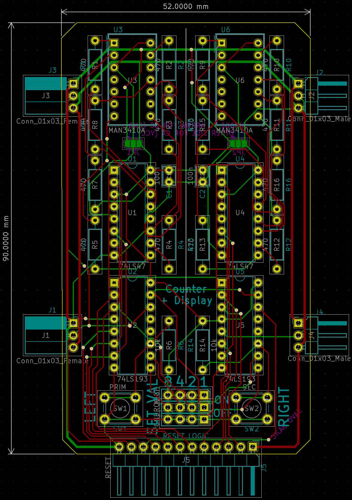
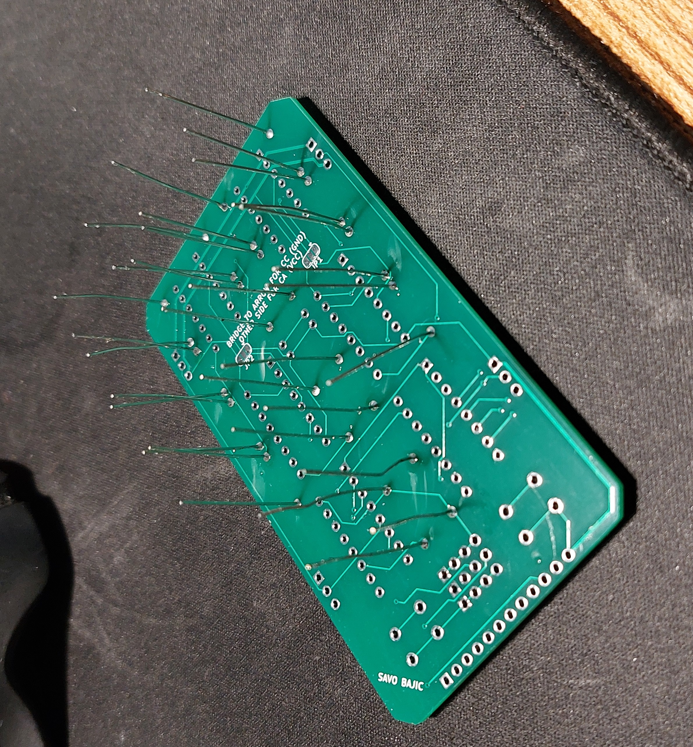
On the back, hidden from most observers is where the solder jumper is to set depending on if a digit is either common anode or common cathode. There is some text on the rear silk screen to explain them.
Renders
Not usually something I bother posting, but I had them prepared for the GitHub page when I initially uploaded my designs there before I had assembled the real boards so I figured I might as well show them here too.
Assembly
I received the boards at the start of March 2022 and quickly set about assembling the boards. This was my first through hole heavy project that I designed and assembled since my oscilloscope for MIE346 three years before this. So it was a bit odd to suddenly find myself flipping a board and cutting excess leads so much during assembly again.
I wonder if I would be able to roll a balloon across these boards and their uncut leads like a high school physics demo.
Signal Generator Assembly
By far the easiest to assemble. Only needed one for my clock, just over a dozen components, and didn’t have to do any jumpers.
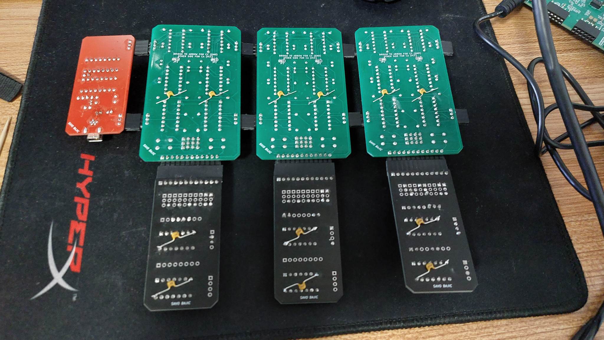
Reset Modules Assembly
These were the easiest base design to solder, with only three components in the schematic. However soldering in the jumpers was a bit tougher than I expected since they moved a bit whenever I would rotate the board to solder them in place.
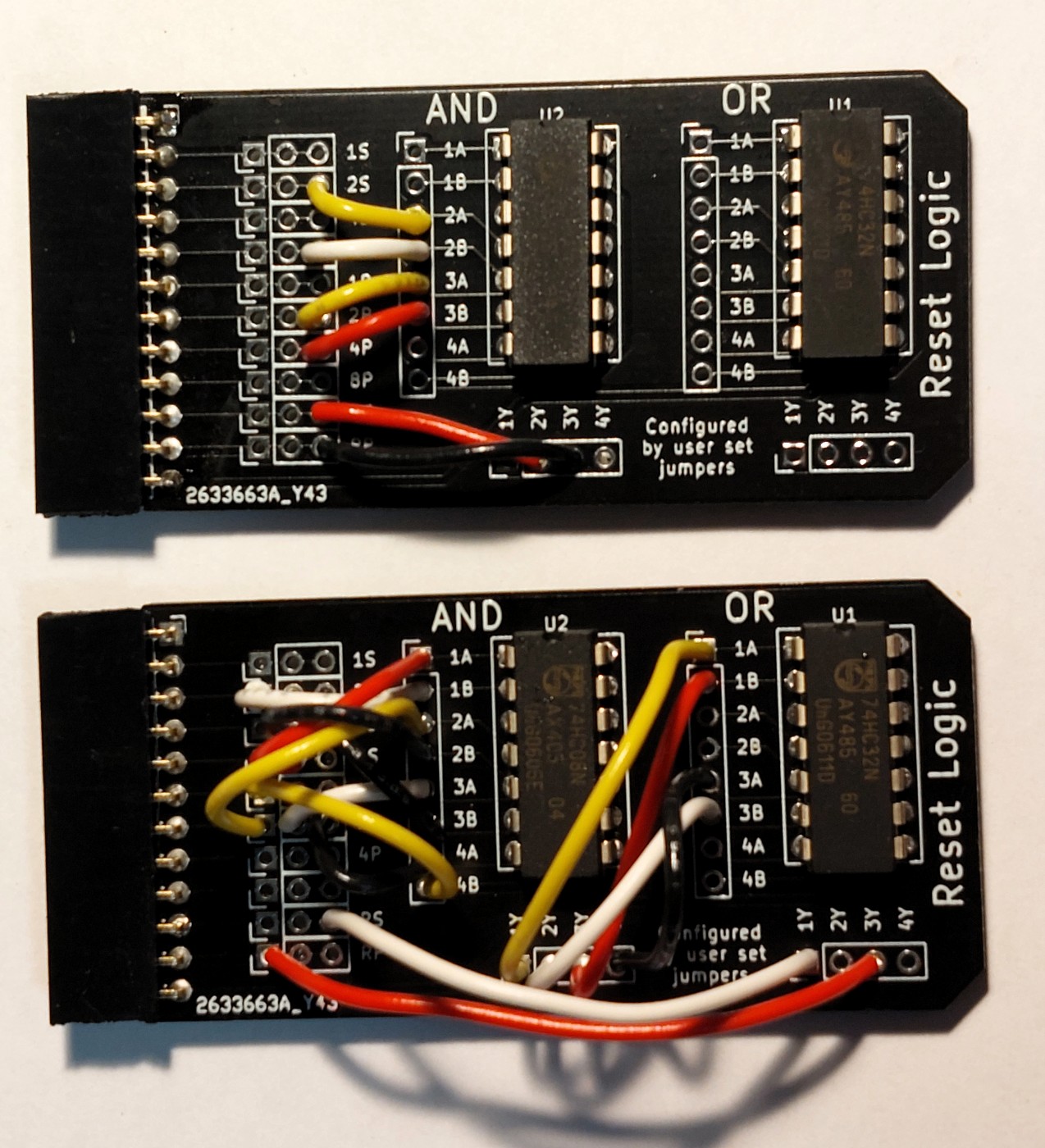
The logic to reset the primary at 6 and the secondary at 10 was pretty simple, each digit only needed a single AND gate. These were needed for the minutes and seconds since they each count up to 60.
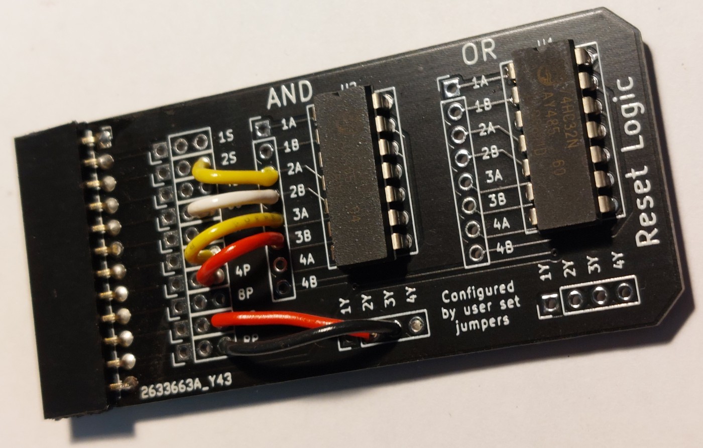
Since I wanted my clock to be a 24-hour clock, for the hours I needed to make a proper 24 reset module. This meant that the secondary would reset at every count of 10, as well as at 4 if the primary is at 2. The primary would reset when it reaches 2 if the secondary is 4, as well as if it reaches 3 in the event it misses the 24 reset and gets incremented anyways. The result is a slightly more complicated logic network.
Yeah a bit more… here’s a (likely redundant) side-by-side.
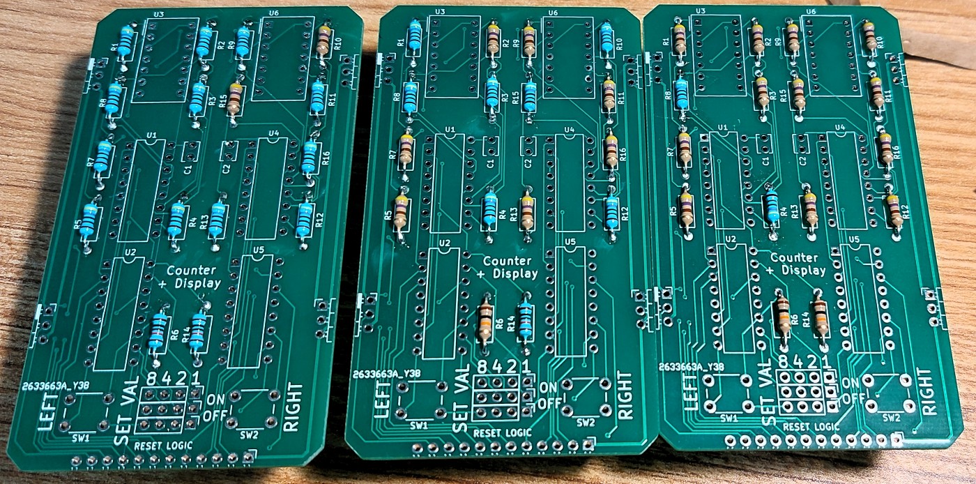
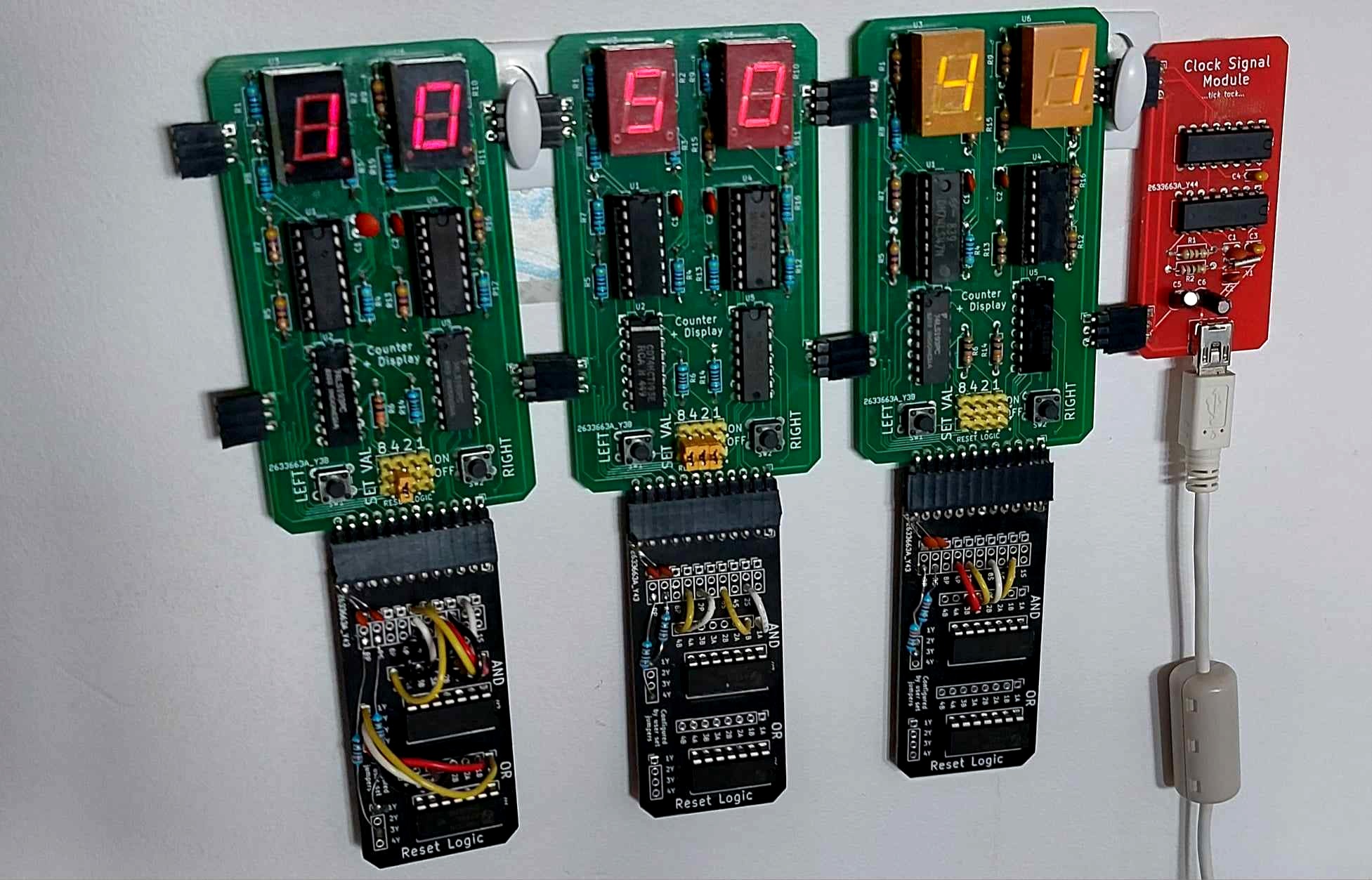
Display Modules
Assembling the display modules went largely by the book. I did diverge from my layout a bit by soldering DIP sockets for the displays and their drivers so I could easily fool around and change them in the future instead of soldering them directly to the boards.
On little artistic touch I ended up doing at a friends suggestion involved my current limiting resistors for the LEDs. I was originally going to only use my 5% tolerance (brown bodied) resistors but realized as I was counting them that I was going to run out of them halfway through making the three display modules I wanted. This meant I was going to need to use some of my 1% (blue bodied) resistors which would throw off the consistency I was looking for. I mentioned this to a friend and they suggested that I set up an ombré (gradient) from one end of the clock to the other with my resistor colours.
The finished module ended up looking like this individually. I noticed that although the sockets add the ability of easy exchange of displays, they now protrude a fair bit from the board, about 12 mm. With the drivers in a socket and the counters directly on the board, it results in a stepped look from bottom to top.
Testing
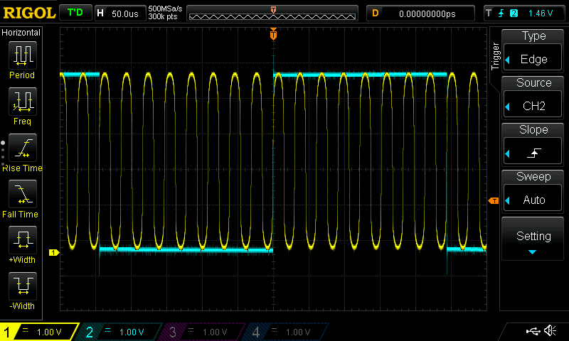
Testing was meant to go in three basic stages. The first stage was checking that my signal generator and power supply module was working as expected. This meant powering it up and checking that it was outputting 5 V properly and a stable 1 Hz signal on the appropriate headers with my oscilloscope, which it did.
The second stage of testing was testing each display and reset module to work as expected. For this I connected each display-reset module pair to keep track of the seconds to see if they kept count well, displayed all the numbers they were meant to (0 to 23 or 59) and then rollover properly. All three pairs worked as needed.
The results of the previous two tests were basically guaranteed since they were copies of what I had done when I was bread boarding the circuits before I committed the design to circuit boards. The real test for the system was “simply” being a whole clock and keeping track of time properly by cascading the counts properly between digits.
Timekeeping Test
So the only real test remaining for the clock to enter service on my walls was to keep time within my desired my desired tolerance of a couple seconds a day. Essentially just a verification.
I was going to leave the clock running and make sure that it was keeping time well, checking it regularly against my phone clock for deviation. It was helpful to use my phone to take photos of it since it would take a time-stamped photo of the clock, which meant I could transcribe the exact time and the clock’s reading accurately and leisurely.
The reason for these checks being regular as opposed to just one after 24 hours or so is that if my clock was not working right I would see if that was due to my reference 1 Hz signal being off, or improper counting resulting in additional or missed rollovers. If the reference was wrong then the difference between each check would be off by a constant factor, e.g. 10% - however if the difference between my clock and the recorded time varied significantly that would indicate a problem with my counting/rollover scheme.
If either of the two issues were to appear, I would prefer the crystal since I would only need to tune one board as opposed to potentially six. It also would be less likely to be caused by a design fault on my behalf and rather component imperfections so I wouldn’t need to alter my designs significantly.
| Real Time | Time Elapsed | Seconds Passed | Clock Readout | Clock Elapsed Time | Seconds Counted | Difference between Clock and Real |
|---|---|---|---|---|---|---|
| 00:41:54 | 00:00:16 | |||||
| 02:02:58 | 01:21:04 | 4864 | 01:21:19 | 01:21:03 | 4863 | -0.02% |
| 09:54:19 | 07:51:21 | 28281 | 09:12:44 | 07:51:25 | 28285 | 0.01% |
| 10:38:36 | 00:44:17 | 2657 | 10:00:00 | 00:47:16 | 2836 | 6.31% |
| 11:46:53 | 01:08:17 | 4097 | 11:10:18 | 01:10:18 | 4218 | 2.87% |
| 13:05:24 | 01:18:31 | 4711 | 12:31:51 | 01:21:33 | 4893 | 3.72% |
| 14:03:17 | 00:57:53 | 3473 | 13:31:43 | 00:59:52 | 3592 | 3.31% |
| 15:32:52 | 01:29:35 | 5375 | 15:01:20 | 01:29:37 | 5377 | 0.04% |
| 16:44:04 | 01:11:12 | 4272 | 16:14:33 | 01:13:13 | 4393 | 2.75% |
| 18:53:01 | 02:08:57 | 7737 | 19:27:31 | 03:12:58 | 11578 | 33.17% |
Looking at this data it is pretty clear that my clock has a stable 1 Hz clock since when it was accurately measuring the passage of time, it was only a second or two off, which very well might have been caused to my photos’ sub-second timing, akin to a rounding error. However, my clock clearly has issues with proper propagation of my roll-over/reset signals.
Investigating the Faulty Counting
The issue is clearly with the roll-over reset logic, but I needed to determine where so I could determine a remedy.
Reset Logic Outputs
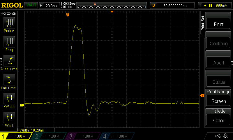
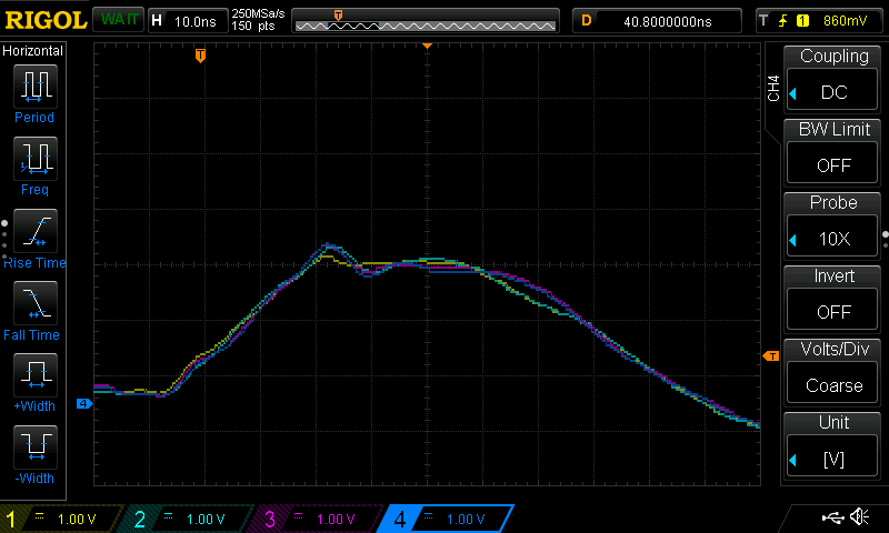
I started by poking around the reset circuitry to see their output waves looked since it is these waves that drive their respective counters to increment or reset. My original suspicion was that these waves might have some noise to them, and if this noise occurred around the threshold voltage the signal might be crossing it several times resulting in these observed additional counts.
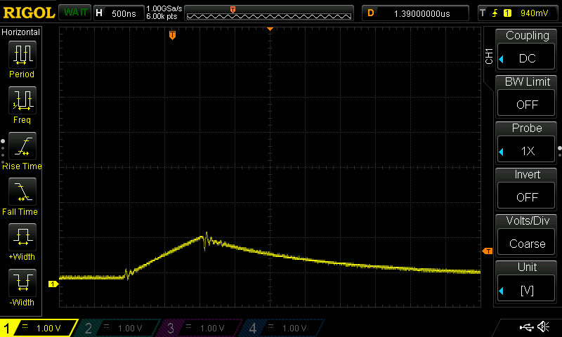
I started by watching the reset signal for each of the seconds digits. The reset pulses were both about 25 ns wide, and swung all the way up to 5 V where they held for roughly 15 to 20 ns. Their lengths were dictated by the feedback delay from the counter and propagation through the logic in all the chips.
The tens of seconds digit’s wave closely resembled the single second’s signal, however it had some leading noise, probably due to some noise induced by the rollover action of the single digit drawing power on their shared boards.

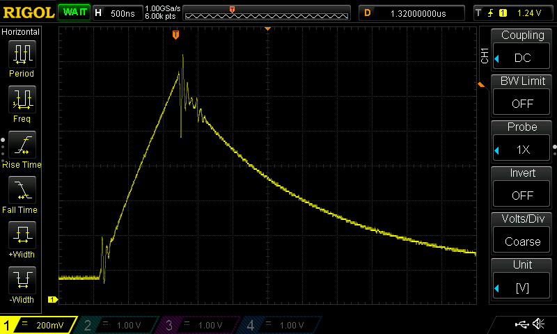
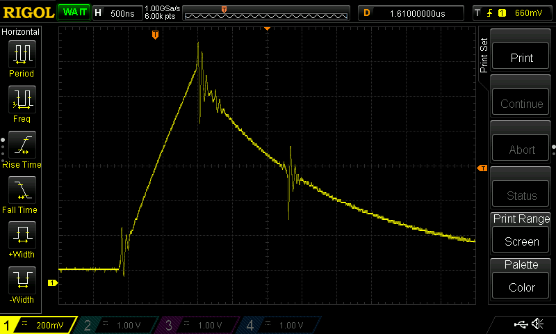
I moved to seeing how the minute reset signals looked. Unsurprisingly they closely matched well with the ones on the seconds display, just with a bit more leading noise. Likely due to the rolling over of the seconds digits.

Even the tens of minutes had similar leading noise to the tens of seconds. Guess that’s evidence of well repeated designs and consistent manufacturing, sharing the same glitches.
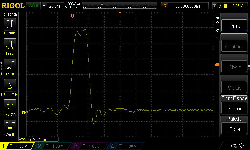
Overall, these waves look acceptable. They are relatively clean square(ish) waves with straight slopes and no observed noise at any intermediate (potential threshold) voltage. They are a bit shorter than I would like but since their length is dictated by the propagation time of the logic that feeds them, I believe this is fine.
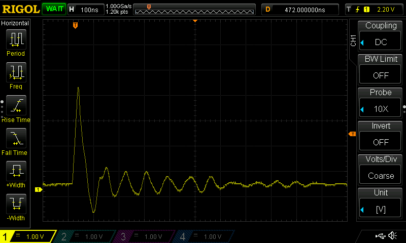
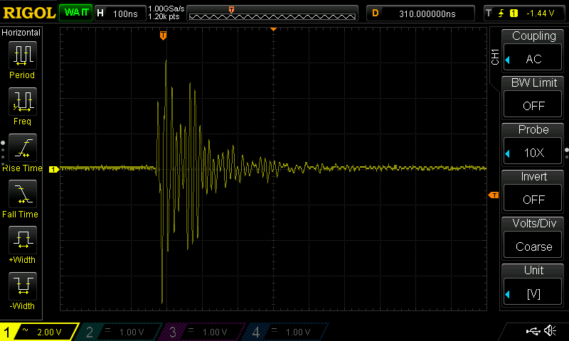
Reset Logic Noise
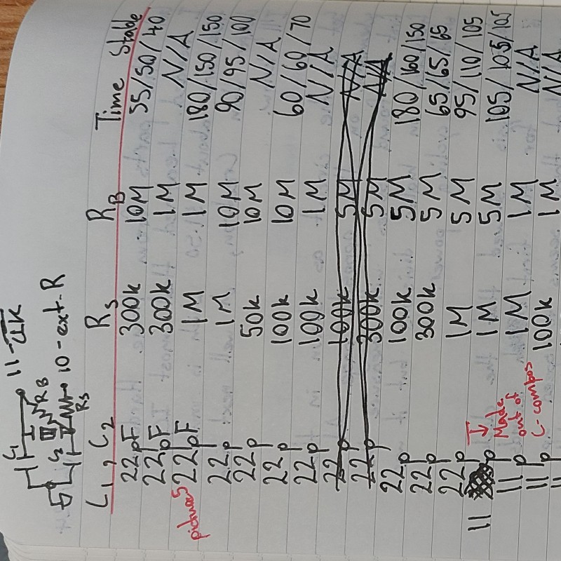
Although the logic signals were relatively clean, when they were at either extreme there is clearly some noise, especially before and after the pulse around ground. I suspected that these oscillations might be enough to mess with the counters so I decided to try out adding some passives to each line to help filter this noise out.
I wanted to design a basic resistor-capacitor low-pass filter. I designed it assuming DC operating conditions, where the capacitor would be charged via a resistor from the output of the logic gate. This was a nice little throwback to my first year circuits class (which ironically actually scared me away from pursuing circuits in the first place!), after digging up my notes I started doing some math.
I figured that a 5 ns charge time would be enough to not impede the function of the clock, but enough to help reduce the noise preceding and following the pulse. Using my spare 47 pF capacitors, I needed to pair them with 22 Ω resistors to get the required response. (I ended up using 33 Ω instead of 22 Ω since those were the closest I had.) So I soldered them in place and… What?
So it turns out I had accidentally over-compensated the system, what I thought were 47 pF were actually 47 nF. Oops. So my response time was only 1000 times longer than intended, but it wasn’t all for naught; I got some neat insights from watching the system with these installed.
- The threshold voltage for counter resets is only about 1 V. I was expecting higher
- The output current of the logic chips is about 50 mA
- The system eliminated any leading trailing noise
- There still were impulses of noise, likely corresponding to the internal switching of the ICs
- Noise around the threshold was certainly a cause for additional counts.
- With these components in place basically every time a digit incremented there was a 25% chance it would increment more than once.
Watching it for some time I observed repeating but uncommon noise on the falling edge. After some time it came to me, these reset signals were captured on the single seconds, this second set of noise happened whenever the tens of seconds rolled over. The timing between this last impulse and the one that precedes it (the peak) is almost identical to the period between the first two periods. When the minutes digits rolled over I would see additional trailing impulses, although smaller in magnitude the further they were.
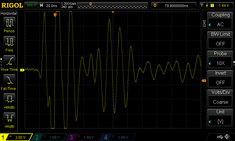
I did source myself some 47pF capacitors and replaced the 47 nF ones. The resulting wave was quite different to either of the previous cases. It eliminated the leading noise but seemed to result in significantly worse trailing noise. It did climb higher, peaking at about 4 V before plummeting back down.
Although much more stable than using the 47 nF, it still wasn’t the solution I needed. My tests with this setup yielded similar results to the system without the passives present, honestly a little worse.
Propagation Issues?
Honestly I wasn’t really expecting the RC filter to fix the issue. I was hopeful though, and I feel it was still a neat little set of experiments.
My current belief is that this issue has to do with the propagation of the short, only 20 ns long, pulse generated. 20 ns is essentially 50 MHz! So not exactly high speed data but still pretty darn quick especially compared to any of my work up to this point. So perhaps I am about start entering the realm of actually having to design for my signals (outside the couple times I put USB connectivity on boards).
One thing I realized looking at my data that all the additional counts seemed to happen on only on the secondary counters, the single digits, and not on the seconds. The only difference between the way these receive their increment signal compared to the primary displays’ counters (tens) is the length and routing of the trace from source to them.
The signal for primary increment (secondary reset) is a single path and is slightly shorter than the trace from the source to the reset for the secondary. This means the signal to increment reaches it before the counter is reset so it will always tick forward correctly.
The secondary increment (primary reset) signal trace is much more complicated and long. First difference is that this signal splits and rejoins thanks to me routing it through both headers used to connect neighbouring modules. This I think is one issue. The other difference/issue is that the route to reset the primary counter triggering this signal is the shortest, both paths to the secondary counter are longer, which means that cascaded counter will experience the same pulse length as the one getting reset (the primary counter gets a little more time with the reset signal being high).
Note: both feature extended vertical runs on the bottom under a trace on the top.
I feel that the big issue is the forking and rejoining of the signal to the secondary, especially since one path is notably longer than the other. What I think is happening is that pulse that goes down the shorter path reaches the counter and triggers a count and then its end starts to arrive and it begins to fall, at which point the signal that took the longer route begins to arrive and adds to it raising it. This occasionally happens around the threshold, which results in the signal appearing as a second pulse.
The longer path is about 110 mm longer than the short one, dividing this by the speed of light/electricity suggests a difference of only 0.363 ns in arrival times. However with slewing, power division, and whatever else goes into high speed communication this might mean more than it sounds like for a 23 ns signal. I’ll see if probing multiple points along the line can give me a better idea of if there are propagation issues.
It didn’t. There is basically no major difference between the signals. The only minor difference is that the signals that were probed further from the capacitor had a bit more swinging to them after the rising edge compared to the “base” signal probed at the capacitor (yellow).
So what now?
Extend the Pulses?
The only thing left that I think can remedy this issue is lengthening the reset pulse and ensuring that it swings the full voltage range. Essentially this means uncoupling it from being directly driven by the logic, and instead just triggered by it and driven by additional logic. Sound like a job suited for the 555!
Before I get cracking on trying this, I need to set a proper baseline number of additional counts. Also find a method of running accelerated tests since I don’t want to wait a day to get results.
To do accelerated tested I could use my function generator to pipe in a higher frequency base clock than 1 Hz. This however has the issue that I can’t use another clock to spot issues anymore (unless I use some specific multiples, but still). So I wanted something more automated that I could leave unattended and it would keep track of failures.
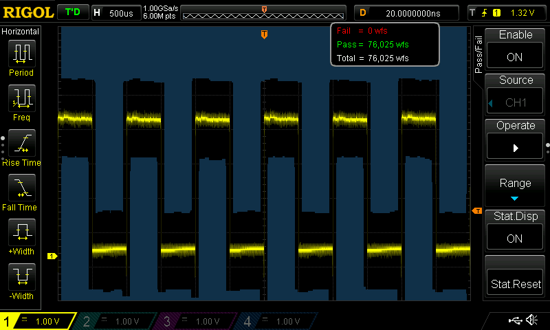
Test Mode on my Oscilloscope
I knew my oscilloscope (a Rigol DS1054) had a Pass/Fail feature included, but I had never used it. After reading the manual I was ready to try it out. Basically the way it works is that you feed your oscilloscope the expected output waveform on a channel, you then set tolerances horizontally (timing) and vertically (value) around the wave. Once set a “no-go” or “rejection” region is set around this waveform.
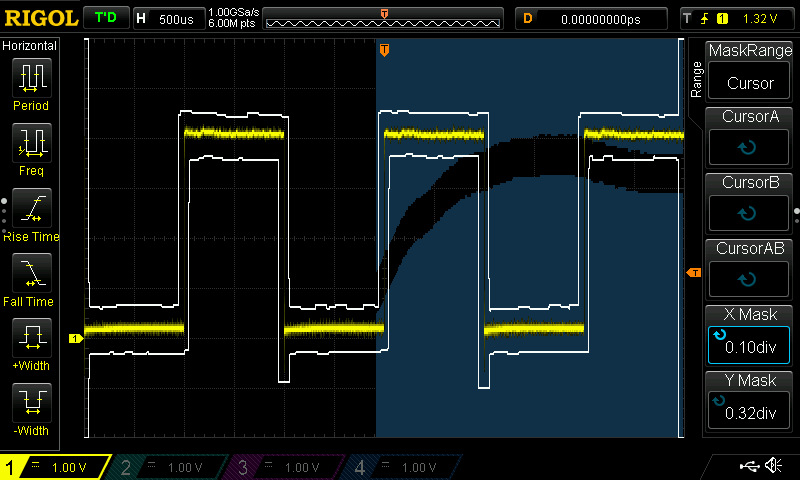
Should any future waves enter it these regions, the oscilloscope records a failure and can stop to record and display the offending wave sample if desired.
For my tests I set the oscilloscope to probe the ones digit of the counter since it alternates state with each count. If a double count occurred, it would be immediately visible. I let the oscilloscope run for some time as I fed the clock an input of several kilohertz. Over time it gradually started to catch some errors.
These errors were however much less frequent than I had observed previously when I let the clock run on its own, only once every 2500 waves. With about 24 counts per waveform on screen, this is implying a glitch once every 60 000 counts/minutes! This is far from the roughly hourly glitches it was having under observation. So I’m glad I have this baseline. Perhaps the probes are somehow scaring the system to work?
Perhaps the glitches are too fast for the oscilloscope to catch at this time base. I’ll do some more runs soon.
555 Time(r)!
So I went ahead and made a 555 timer circuit for this purpose, a mono-stable 555 with an approximately 50 microsecond pulse length. This should be long enough to register on any chip. I used components I had laying about, I probably could have used a shorter period or smaller capacitor but this should work.
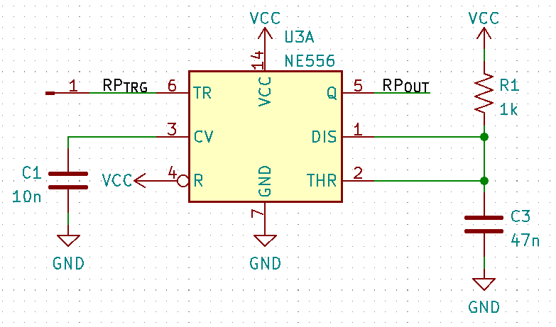
One issue I noticed immediately was that it was basically constantly firing off pulses. I had forgotten that the 555 takes in “negative” logic for the trigger, so it is triggered when it the trigger pin is pulled low. This is the inverse of what my reset logic outputs so I had to throw in a basic inverter to handle this.
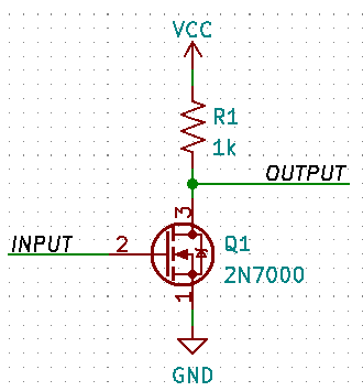
Originally I used a 10 kΩ resistor to pull up the output but the output charged too slowly so multiple pulses were made, so I reduced it to just 1 kΩ. After some more basic tests, my test bread board was ready to get inserted into the system.
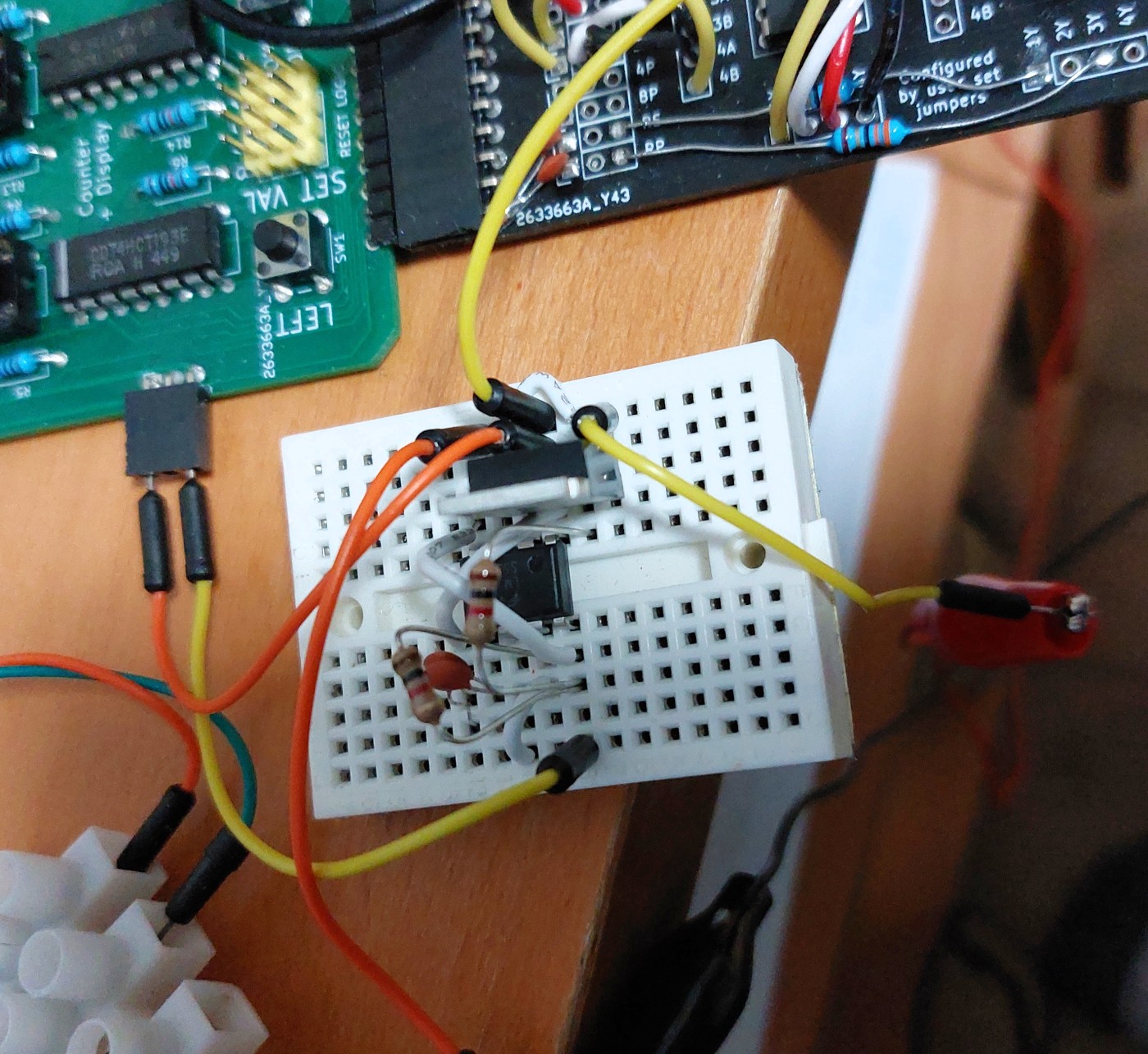
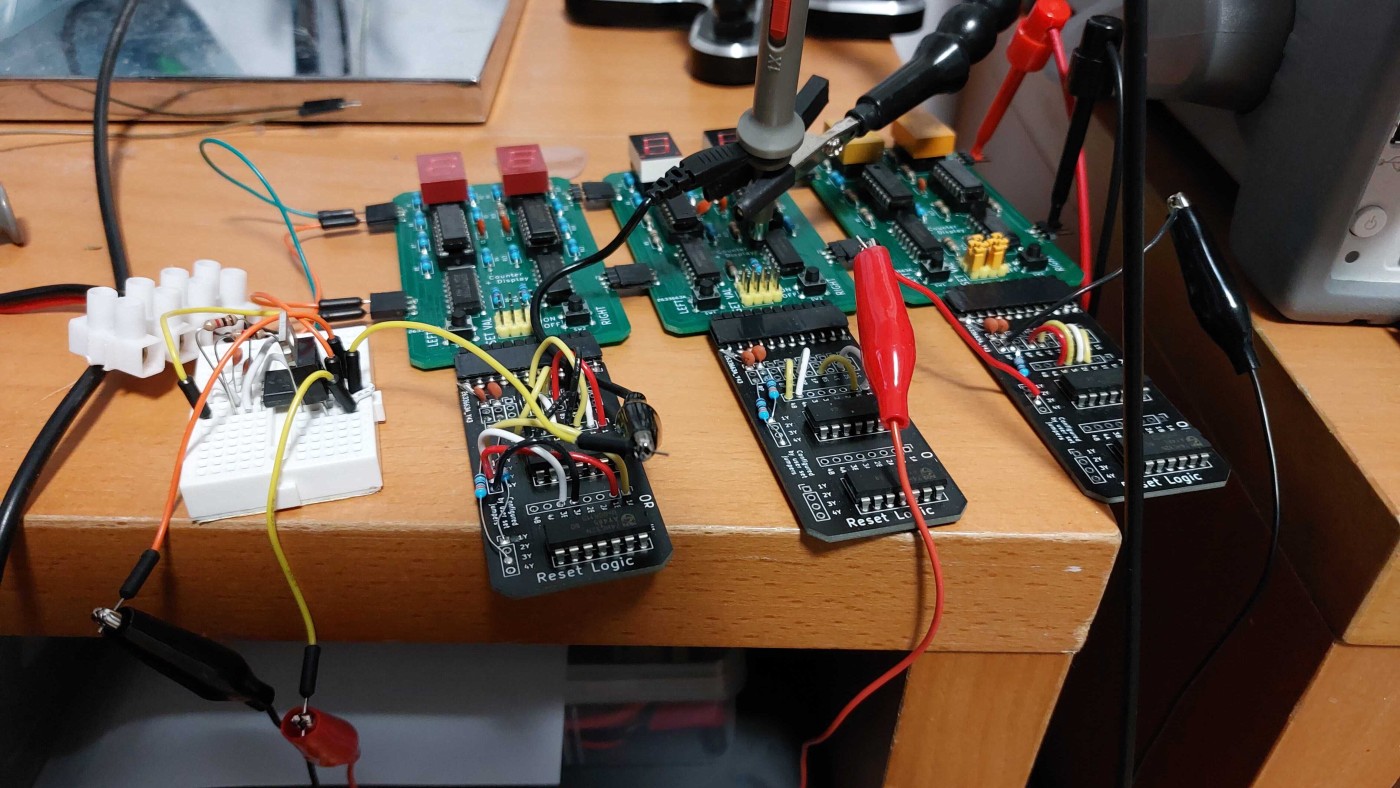
I wired the input of the inverter to the usual logic that would reset the primary digit and increment the secondary above it, and then the output to the RP header of that logic board, thus it intercepted and inserted its own reset pulse.
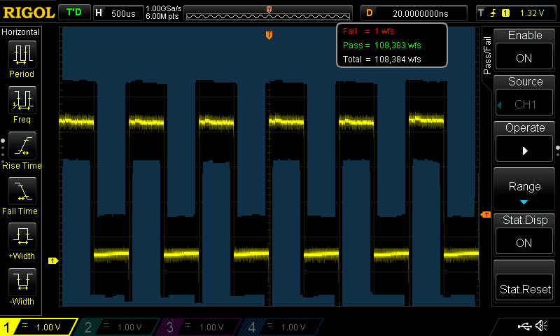
Speed Testing the 555
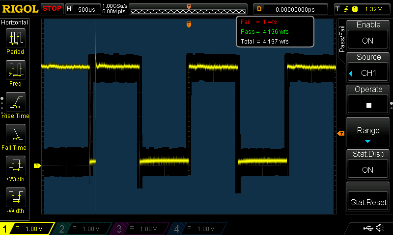
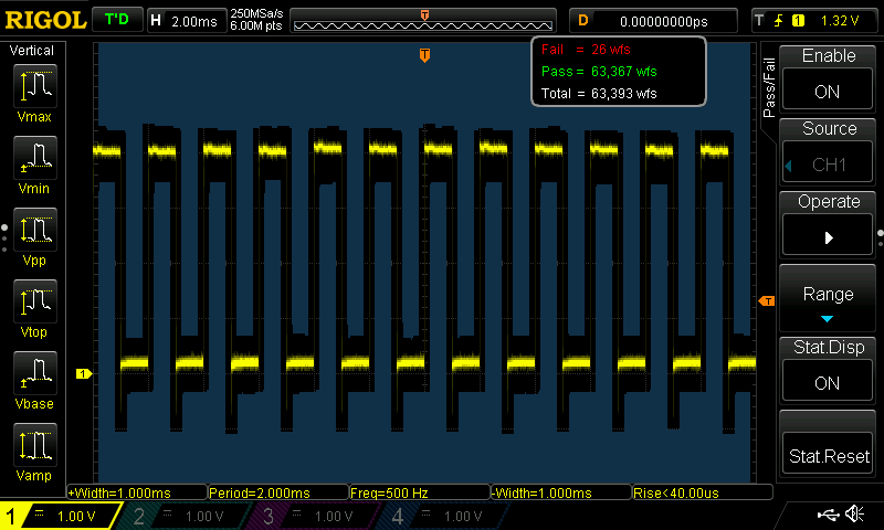
With the 555 timer circuit installed I began feeding the system a controlled reference clock from my function generator. The test started excellently. I turned up the function generator to run a 120 kHz base clock and left it running. I checked in on it periodically for any recorded failures.
Amazingly no failures were detected in the first almost 80 thousand waves, which was 960 000 simulated minutes! I kept it going and accidentally brushed up against my table which I think created a measurement glitch.

In the end though after almost 110 000 waves with only one recorded failure, I ended the test. This was equivalent to 1 300 596 minutes, or just under 2 and a half years! Even this one failure was likely my fault rather than a genuine circuit issue.
Proper Testing of the 555
Although the results look promising from these accelerated tests, I will conduct a test of just letting the clock run normally. My reason is that when I was doing these accelerated tests, there were significantly less frequent extra counts caught on the original hardware (1 in 2000) than when I had it running off the signal module (roughly 1 in 100). I don’t know why this is for certain; perhaps the supply is more stable from the my power supply than my computer’s USB port, or maybe the probes affect the board slightly and it works better as a result. Anyways, I want to repeat my original, authentic use case test to have a proper verification. Since I only have the 555 timer for the ones of minutes digit, I will disregard an glitches on the ones of hours.
| Real Time | Time Elapsed | Seconds Passed | Clock Readout | Clock Elapsed Time | Seconds Counted | Difference between Clock and Real |
|---|---|---|---|---|---|---|
| 01:35:49 | 00:00:14 | |||||
| 02:26:43 | 00:50:54 | 3054 | 01:21:19 | 00:55:41 | 3341 | 8.59% |
| 08:26:53 | 06:00:10 | 21610 | 06:56:11 | 06:00:16 | 21616 | 0.03% |
| 08:58:15 | 00:31:22 | 1882 | 07:27:33 | 00:31:22 | 1882 | 0.00% |
Well shoot. Looks like the 555 wasn’t the silver bullet I needed. What I am beginning to suspect is that it is indeed issues with my power supply. Until now I have been testing using my computer’s USB port to supply power. Clearly it has been capable of supporting the clock and its power draw that can reach up to 300 mA at 5 V, however the varying power draw of my computer itself and the clock as it changes digits is probably causing some noise on the power line and thus glitched counts.
This is why when I left the clock running overnight in both this test and the previously listed one, there was basically no miscounts. I was asleep and my computer was off, so the only thing drawing power was the clock. When I was awake and using my computer, that’s when the issues began. To test this out I’ve moved the clock to have its own power supply, independent of my computer and will be checking its ability to keep time.
That being said, I still believe the 555 is a good addition since the pulses were just long enough to trigger a reset previously. So having the 555 time independently likely brings some stability, although I could do another test where I just don’t have the 555 but have it running off its own supply if this supply test comes back with good results.
| Real Time | Time Elapsed | Seconds Passed | Clock Readout | Clock Elapsed Time | Seconds Counted | Difference between Clock and Real |
|---|---|---|---|---|---|---|
| 09:15:30 | 00:00:17 | |||||
| 09:55:55 | 00:40:25 | 2425 | 01:09:26 | 01:09:09 | 4149 | 41.55% |
| 10:33:33 | 06:37:38 | 2258 | 02:12:15 | 01:02:49 | 3769 | 40.09% |
| 10:44:38 | 00:11:05 | 665 | 06:07:35 | 03:55:20 | 14120 | 95.29% |
Yep, definitely a power issue.
Power Issue
Looking at the disappointing data from the standard USB supply’s power I determined that this is definitely going to need a revised power delivery system. After this I left the clock running but put a probe to monitor the 5 V line for noise and observed massive amounts of noise around when there would be digit changes, especially when these changes had glitched and we accidentally had extra counts.
That’s not great, probably causes some glitches.
Oh jeez this isn’t good.
…$%#@%!
So clearly this system has some issues. Since the main power draw are the displays since each illuminated segment draws roughly 6.5 mA, so I figured I can try to see where the most change on power draw occurs in the system to predict these issues, as well as recreate them better.
| Digit | Number of Segments On | Change from Previous (0-9) | Change from Previous (0-5) |
|---|---|---|---|
| 0 | 6 | +1 | +1 |
| 1 | 2 | -4 | -4 |
| 2 | 5 | +3 | +3 |
| 3 | 5 | - | - |
| 4 | 4 | -1 | -1 |
| 5 | 5 | +1 | +1 |
| 6 | 5 | - | N/A |
| 7 | 3 | -2 | N/A |
| 8 | 7 | +4 | N/A |
| 9 | 5 | -2 | N/A |
Looking at this and knowing the behaviour of the clock (being a 24-hour clock) I know that the most segments change going from 09:59:59 to 10:00:00, a total of 9 segments change - however the net change in power draw is only 1 segment’s worth. The largest change in power draw is going from x7:59:59 to x8:00:00, where x is either 0 or 1. This has an increase on the power draw worth 8 segments, which when going from 17:59:59 to 18:00:00 is an increase of 32%! These sharp changes in power draw (up to 32%, 52 mA) are likely the issue.
What can I do?
Well I have a couple options I can use to try and address this issue:
- Tune the capacitors on the power supply board.
- They might need to be increased to help deal with this ripple
- They might need to be decreased since the supply might not be as capable of driving such a capacitive load
- Get a better USB power supply
- My current one is rated for up to 2.5 A though.
- I could use my spare desktop supply
- Surrender myself to not fixing this issue and transition to making this a piece about the immaterial nature of time
- Compete to make the first broken clock that is right three times a day
At this point I’m leaning towards trying a bit of 1, before deciding between either of 3 or 4. I will probably start by reducing the capacitance and then build it up until it .
Thunder Stuck
I removed the capacitors from the signal/power board and plugged it in. I checked that the oscilloscope was good and monitoring the voltage lines for noise, then plopped down in my office chair.
Zap
I received a static shock, not usually notable - BUT I saw that at that instant noise similar to what happened before was recorded on the oscilloscope. It clicked. I started scooting around in my seat and was able to generate more noise as I pleased, I could even watch the minutes skip forward as I did!
It all made sense looking back:
- Static shocks can only occur when I am around, hence the solid night operation
- The noise was massive, I doubt even a faulty power supply would be able to swing 40 V like that
- The minutes were the main digits effected in this test due to the long wires picking up EMI
- I was wearing different pants than I was previously. (Yay laundry!)
- I know that the ones I was wearing then had a habit of generating shocks all winter
- The ones I was wearing when doing the 555 tests didn’t give me as many shocks
- This explains the decreased baseline glitch frequency in those tests
- I recall wearing the offending pants back when I first assembled the boards, and first noticed the glitches
- The weather was dryer compared to the previous few days when I was testing
Revisions
I plan to keep the 555 as part of the design. Also need to work some EMI hardening, ideally without needing to remake the display modules. Maybe I can cut the top signal traces so they only get passed through the bottom inter-connects?
Revised Reset Module
I’ll incorporate the 555 timers into the reset module, using a 556 chip to provide two separate 555s to drive a pulse for each of the digits per display module. In addition to this 556 timer, I have replaced the OR gates with NOR gates to provide the inverted logic the 555s need to be triggered correctly.

The main difference to the layout is the overall extension of the module to add the 556, as well as changing the trace for the NOR chip from the OR chip it replaced.
This time I specificied to my manufacturer to put the order number on the bottom out of sight.
Since I included the renders of the other modules, why not this one too?
Conclusion
I did end up ordering the 556-based reset modules, however I did not bother to assemble them since I felt that the issue had more to do with a lack of ESD protection across the board. So I opted to add in 100 nF decoupling capacitors for all the ICs that I neglected to include them on since I figured this would harden the entire board against ESD.
This repair seemed to work! I now have it mounted on my wall and it’s been working well. My only comment is that the leftmost digit is a bit dimmer than the others, and using jumpers is not the easiest way to set the time, but otherwise the clock is doing fine and will probably remain as is.
We’ll see if the static issues return in the winter! It’s hard to generate the same level of static in the middle of summer as I write this.
EDIT (2025-01-05): Decoupling capacitors seem to have done the trick, ticking along steady regardless of season or outfit!
Final Comments
If I were to do this again I would properly integrate the decoupling capacitors on the boards. In addition, since I’ve observed the counters having internal pullups on the data load pins I would switch the headers for setting digits to switches that would pull them down as needed to make setting it easier. I originally went with the jumpers since I didn’t want to include pullup or pulldown resistors on the boards.